Summary of Optimizing Performance: A Guide to Stacking Precision Power Supplies
Summary: A modular, low-cost stackable power supply system with a Hub Board and multiple Stack Boards provides precise adjustable outputs (10–20 mV), analog (potentiometer) or digital (USB/I2C) setpoints, CC/CV and short protection per board, and LCD status displays. The Hub enumerates stacked boards, reads setpoints via ADC, and communicates via I2C; each Stack Board contains a buck/boost DC/DC converter, programmable resistor for output, potentiometer, and protection. Safety features include fuses, sense resistors, and zeners; design targets ease of expansion and hot-swappability.
Parts used in the Modular Stackable Power Supply Project:
- Hub Board (main card with AVR ATmega microcontroller)
- Stack Boards (daughter cards)
- 12V DC input source (banana jack or DC barrel jack)
- Linear regulator (12V to 5V for microcontroller)
- AVR ATmega microcontroller
- I2C bus and 8-pin slave select bus
- Multi-turn analog potentiometers (on stack boards)
- LCD screen for setpoints and output display
- DC/DC buck/boost converter chip (Linear Technology LT3112 or equivalent)
- I2C-programmable digital resistor (e.g., 1024-step digital potentiometer)
- Sense resistor for current/short detection
- Zener diode for reverse-voltage protection
- Fuses for short protection
- Resistive voltage divider network for board count sense (10 kΩ resistors referenced)
- Connections/headers for stacking and power distribution
- Serial/USB connection for digital input from a computer
1. Introduction
Statement of Purpose
Our project selection stems from the recognition that power supplies represent a crucial and costly aspect of any electrical project. In an industrial context, numerous product test setups demand precision voltage references, but the acquired supplies often exceed the required wattage and come at a higher cost. Conversely, for hobbyists and students, the expense of a single power supply proves to be a barrier, escalating proportionally with the demand for additional outputs. Our emphasis is on the project’s modularity and affordability, addressing key factors vital for both industrial and individual markets.
Objectives
Goals
1. “Create a finely adjustable power source with exceptional precision (10-20mV).”
2. “Enable the vertical stacking of power supply boards without mutual interference.”
3. “Incorporate dual input methods: analog potentiometer and digital programmable line.”
Functions
1. Offer adjustable power output with a precision of 10-20mV.
2. Utilize an input configuration featuring either an analog, tunable knob, or a digital, USB line.
3. Employ stackable boards equipped with short protection to prevent malfunctions affecting other boards.
Benefits
• Expand affordably with boards that come at a very low cost when stacked.
• Enjoy a straightforward system with easily understandable settings for input/output, CC/CV, and analog/digital setpoints.
• Experience the convenience of “hot-swappable” boards, thanks to short protection, eliminating any risk to other stacked boards or the hub board.
Features
1. A modular system featuring minimal expansion costs, with boards priced significantly lower than commercial alternatives.”
2. “In the worst-case scenario, the short protection circuitry guarantees that only a singular header board will be affected.”
3. “An LCD screen indicator that displays all settings, including analog/digital input and CC/CV modes.
2. Design
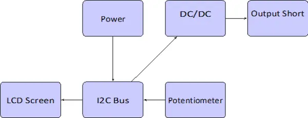
System Diagram
System Overview
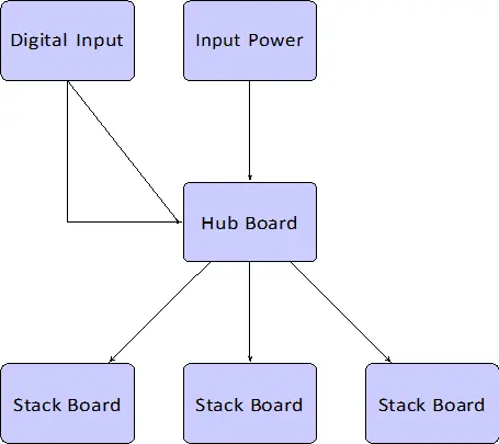
From a technical perspective, the system is structured based on a concept involving a main card accompanied by additional attachable daughter cards. To ensure a coherent syntax, we designate the main card as the “Hub Board” and the attached daughter cards as the “Stack Boards” consistently. The Hub Board is responsible for receiving inputs from diverse sources and transmitting them to the Stack Boards. Each Stack Board is equipped with its own DC/DC converter to configure the output.
Input Power
The entire system is designed to be powered externally through either a banana jack or a DC barrel, delivering a 12V DC supply. The required wattage for this power source should be relatively high, as it must support all the stacked modules in the system. Our estimate suggests that a peak power of up to 15A may be necessary.
Digital Input
Setting the stack boards’ set points can be accomplished through a digital input stream, representing one of the two available methods. This process involves a computer executing a script to open a serial port. The microcontroller communicates the number of boards, prompting the computer to request set points for each board. Once this information is gathered, the system stops seeking input and displays the confirmed set points along with their corresponding actual output values.
Hub Board Overview
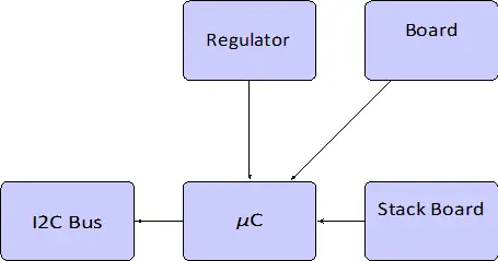
Regulator
The entire board operates on a 12V DC power supply, but since our microcontroller requires 5V DC, we will utilize a linear regulator to step it down.
Microcontroller
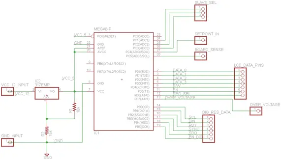
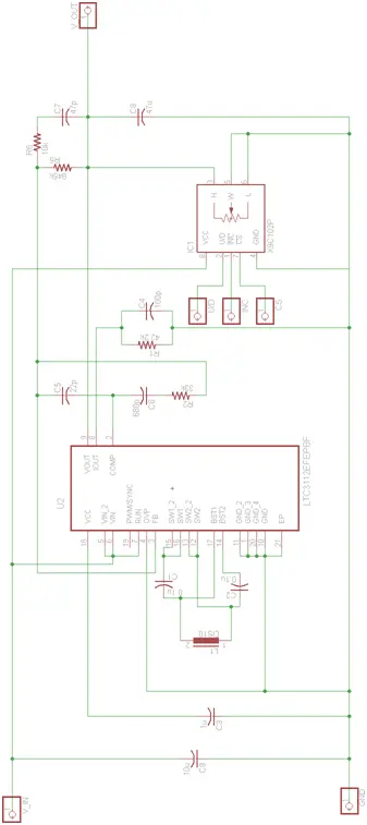
In our project, we will employ an AVR ATmega microcontroller as the central component. The power supply will be derived from a regulator. The microcontroller’s task involves tallying the number of boards and subsequently acquiring the potentiometer set points from each stack board. Utilizing this information, it will compute the required output values for each converter chip. The calculated data will then be transmitted via an I2C bus to each stack board, along with the necessary datastream for the LCD screen. Figure 3 illustrates the configuration of the microcontroller circuit, where the input originates from the power supply and board sense circuitry, while the output is directed to both the I2C bus and the LCD screen bus.
Stack Board Setpoint
The potentiometers will be physically positioned on the stack boards, transmitting voltages to the hub board. These voltages will then be processed by the microcontroller through an ADC. It is crucial to guarantee that our ADC possesses sufficient precision to accurately distinguish between minor voltage levels, typically in the range of 10mV.
I2C Bus
The microcontroller computes various data, such as set points, calibration values, and LCD screen bits. This information is then transmitted from the microcontroller to an I2C bus to facilitate communication between boards. Employing an 8-pin slave select bus configured as active high, we utilize the slave select bit to handle all data streams, ensuring that communication occurs with only one board at a time.
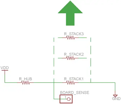
Board Count Sense
To tally the board count, our strategy involves employing a microcontroller to interpret a voltage established through a resistive voltage divider. A constant fixed resistor, affixed to the hub board, constitutes the upper end, whereas the lower end comprises a parallel arrangement of resistors from the stacked boards. The addition of a stack board will reduce the resistance by a factor corresponding to the number of stack boards. The resultant intermediate value will be directed to the ADC line. Initially, we considered utilizing a 5V supply voltage; however, it proved insufficient to afford the ADC the necessary range for precise discrimination. To express it mathematically:
VLSB = VDD/210 = 5/1024 ≈ 5mV
Featuring a 5mV Least Significant Bit (LSB), the ADC maintains precision across various ranges. This specification establishes the allowable resistances for our setup.
Rstack/8 Rstack/7 0.005
. Rtop + Rstack/8 Rtop + Rstack/7 . 10
Given this, we can opt for a resistor ratio that enables us to detect this slight variance. The choice of 10kΩ resistors was deliberate, aiming to reduce power dissipation along this pathway. By fixing Rtop at 10kΩ, we systematically varied the resistor ratio to identify the maximum voltage differential.
The ideal ratio is established at 0.3518. By employing this ratio, we can graph the output voltage corresponding to each extra board.
The minimal variance is evident between the 7th and 8th boards, amounting to 133mV or 26 LSBs, comfortably falling within our acceptable accuracy range.
Stack Board Overview
Power
The daughter boards receive their input power by tapping into the 12V DC line transmitted from the hub board.
DC/DC Converter
The pivotal element on the stack board is the converter chip, functioning as a buck/boost switching DC/DC regulator. In the existing designs, the preferred choice is the Linear Technology 3112, capable of delivering DC voltages within the range of 3-15V [2]. To establish the output voltage, a resistor ratio is employed through a conventional non-inverting amplifier arrangement. This ratio adjustment is achieved by incorporating an I2C-programmable resistor, facilitating precise configuration for accurate output values. The formula governing the adjustment of the output voltage is as follows:
Vout
= 0.8V · 1 + R1
According to the datasheet, it is advised to use resistors with values in the order of kilohms or higher to reduce power wastage. To attain the desired voltage range for a stacked board, we sought a highly precise digital resistor capable of covering an extensive range. By employing a 1024-bit digital resistor [3], with R2 set at 4kΩ and R1 sweeping from 0 to 50kΩ, we can calculate the ultimate precision in terms of least significant bits (LSBs):
∆Vout
∆Rdig
= 15 − 3 = 0.24mV <<< 1 LSB
50k
While possessing this is beneficial, another crucial precision measurement involves determining the variance between steps. For instance, setting values at 782 compared to 783 would result in what variance in voltage output? Given our selection of a linear output, we can compute the difference in a linear fashion:
∆Vout = Vout(X + 1) − Vout(X) = 9.8 mV ≤ 1 LSB
Meeting this specification poses a greater challenge, given that a 10-bit digital potentiometer appears to be the upper limit in precision. Although it is just slightly below one LSB, the selected component should suffice for our design.
Figure 6 illustrates the internal converter of stackable modules along with its connected peripherals. The output is configured through a resistor divider, which can be fine-tuned using an I2C programmable potentiometer. If desired, supplementary circuitry around this foundational circuit can introduce multiples of 12V as a bias, thereby expanding the potential voltage range of the overall design.
I2C Bus
Refer to Section 2.2.4
Potentiometer
For its intended purpose, the potentiometer must possess both high precision and linearity. Additionally, it will be designed as a multi-turn potentiometer to enable users to make more refined adjustments.
LCD Screen
The LCD screen will showcase the present set points for the board, along with the real-time output values in both voltage and current. Additionally, it will include an indicator to denote the presence of a shorted output on the board, also recognized as the CC/CV mode indicator.
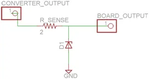
Output Short Protection
We aim to guarantee the safety and stability of our circuit in the presence of a short or reverse polarity output. To address these concerns, we employ two distinct methods, each tailored to its specific scenario. For short circuit protection, a sense resistor is integrated into the output circuit to monitor and prevent excessive current draw. In the event of a short circuit, the rapid increase in current causes a corresponding rise in voltage across the sense resistor. By measuring this voltage, we establish a VOV (Voltage Over) threshold, and if surpassed, it triggers the shutdown of the chip. The microcontroller utilizes an ADC pin to measure this level and initiate the shutdown process for the specific converter chip. In addition, to safeguard against reverse voltage, we implement a zener diode in parallel with the output.
In Figure 7, we show the layout of our simple over voltage protection circuit.
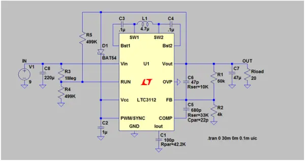
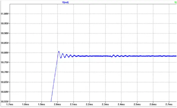
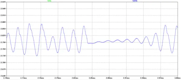
Simulations
The converter utilized, as outlined in Table 4, was accompanied by an LTSpice file for the validation of our designs [2]. Our testing encompassed both ends of the converter, and the corresponding plots are presented below.
Flow Charts
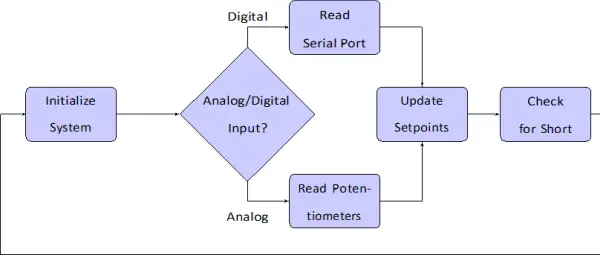
At the highest conceptual level, this system promptly responds to user-input adjustments related to output voltage and maximum output current. The system’s responsiveness is limited only by the processing capabilities and clock speed of the microprocessor. Upon activation, the system undergoes an initialization phase during which the hub board assesses the number of connected boards by examining the impedance of the sense line at the output. In non-hub modules, the sense line contains predefined resistor values, facilitating the microprocessor’s enumeration of connected boards. Subsequently, the LCD screen is cleared to eliminate any previous values. The LCD screen updates once the initial setpoints are transmitted to it.
The user then selects the desired input control method (analog or digital) by flipping a switch, determining the approach for adjusting voltage setpoints and current limits. Depending on the user’s choice, the system reads either the analog input from potentiometers or digital input from a serial port. The internal microprocessor then modifies programmable resistors that govern the corresponding thresholds, directly linking them to the feedback loop of the DC/DC converter ICs. A system check for shorts is conducted, triggering an immediate shutdown if detected. This safety stage incorporates dual protection layers, including a fuse and a feedback loop from the controller to the internal converters.
Tolerance Analysis
Counting the stacked modules connected to the hub stands out as a crucial aspect of our project. This involves establishing a sensing path with resistors that will be parallelly stacked, forming a voltage divider circuit for the microcontroller on our hub board to interpret. Given the microcontroller’s confined 0-5V range, it’s imperative to ensure a high precision in the Analog-to-Digital Converter (ADC) to accurately identify the number of boards. This task becomes challenging swiftly as more sense resistors are added in parallel, causing each subsequent board to have a diminishing impact on the overall resistance.
Assuming a maximum of 8 boards in the stack, the discernible difference between having 7 and 8 boards is approximately 20mV. The microcontroller’s ADC is 10-bit, implying that one Least Significant Bit (LSB) corresponds to 5mV. If the resistors have a 10% tolerance, the 20mV difference transforms into a 7mV difference at the worst case. This shift turns a seemingly straightforward 4-bit change into a considerably more intricate 1-2 bit alteration, making it challenging to distinguish from background noise. Moreover, variations in temperature, especially in our high-power and compact system, can impact resistance, further contributing to the observed fluctuations.
4 Safety
In adherence to the IEEE Code of Ethics, it is imperative to identify potential hazards to users and take preventive measures whenever feasible. Instances where precautionary actions or user notifications are warranted include situations involving shorting terminals, usage of inadequately rated power sources for input, and overloading the converter.
For the first scenario, preventive steps will be implemented against short conditions in each module, incorporating a fuse and a zener with standing load. This dual approach ensures the avoidance of part derating and the risk of fire due to excessive current. Users must also be informed of the necessary specifications for the input power source to prevent issues such as blown fuses and improper operation of converter modules resulting from drawing more current than the source can handle. Lastly, users need to understand the capabilities of each stackable module. While voltage settings are confined to a specific range for each converter, knowledge of the maximum current drawn by external circuitry is essential before utilizing the module. Failure to do so may lead to unintended consequences in the external circuitry, particularly when our current-limiting system is implemented.
- How precise is the adjustable output?
The design targets precision of 10–20 mV as stated in the objectives. - Can boards be stacked without interfering with each other?
Yes; the design enables vertical stacking with per-board short protection to prevent mutual interference. - Does the system support both analog and digital setpoint inputs?
Yes; setpoints can be provided via onboard potentiometers (analog) or via a digital USB/serial input (digital). - What converter chip is used on the stack boards?
The document references the Linear Technology 3112 (LT3112) buck/boost DC/DC converter as the preferred choice. - How does the hub detect how many boards are stacked?
The hub measures a voltage from a resistive divider formed by fixed Rtop and parallel resistors on each stack board, read by the ADC to count boards. - How is short-circuit protection implemented on each board?
Short protection uses a sense resistor to detect overcurrent and an ADC-monitored threshold to trigger shutdown, plus a fuse and a zener for reverse protection. - Can the output voltage be programmed remotely?
Yes; the microcontroller computes outputs and sends I2C commands to programmable resistors on each stack board to set the converter output. - What is shown on the LCD screen?
The LCD displays setpoints, actual output voltage and current, and an indicator for CC/CV or shorted outputs. - What supply voltage powers the overall system?
The system is powered by an external 12 V DC supply connected via banana jack or DC barrel. - What limits the system responsiveness to user adjustments?
Responsiveness is limited by the processing capability and clock speed of the microcontroller.