Summary of PIC Microcontroller Development Board System
This project describes a flexible PIC microcontroller development system using a two-PCB approach: a main backplane hosting power, reset, RS232 and programmer headers, and removable standardized daughter boards for various PICs and peripherals. The system routes 43 I/O lines, SPI (with five CS lines), I2C, UART/RS232/RS485/MIDI, USB D+/D-, and programming lines across two 2x30 pin headers. Multiple daughter-board Gerber files and KiCAD libraries are provided to support custom peripherals and controllers, enabling interchangeable, space- and cost-efficient prototyping.
Parts used in the PIC Microcontroller Development Board System:
- Main back plane PCB (power supply, MCLR reset, RS232, PICKIT header)
- Daughter board PCBs (standardized footprint)
- Two 2 x 30 2.54mm pitch pin headers
- Power supply components (VDD, GND)
- MCLR reset components
- PICKIT programmer pin-header
- RS232 interface components
- SPI bus lines and 5 SPI Chip Select lines
- MOSI, MISO, CLK wiring for SPI
- I2C bus shared on SPI wiring
- Dedicated TX and RX lines for RS232/RS485/MIDI
- Dedicated D+ and D- lines for USB
- PIC programming lines: MCLR, PGD, PGC
- Various daughter modules (examples provided as Gerber files): dsPIC30F modules, PIC16/18 modules (8/14/20/28/40 pin, USB and non-USB), MCP3208 modules
- Peripheral modules: LEDs for I/O 0-39, 12 Bit DAC, Seven Segment, MIDI, PIC ADC, ULN2003, Push Buttons, Switches, 16x2 LCD
- Pin header breakouts
- KiCAD component libraries and footprints
This project is for the design and use of a PIC development tool which is flexible to suit a wide range of PIC based electronic projects.
It is often easier to develop microcontroller projects with the use of development tools; which allow user based code to be demonstrated in real time. However, from personal experience, a number of existing development boards can often suffer from one or multiple of the following limitations;
1. Comprehensive designs are often expensive,
2. Carry very little peripherals,
3. Contain peripherals which are not suited to specific projects and therefore are rarely used,
4. Contain peripherals which occupy a large amount of board space thus adding to the cost,
5. Are unable to be changed or support a change in peripherals,
6. Contain a surface mount processor which cannot be removed and thus limiting the use case of the development board.
In reality, the user often chooses a development board based on the requirements of the project, however, this can lead to a mountng collection of development boards or restrict the freedom of the design.
The PIC development board design presented here aims to expand on these limitations.
The development system makes use of a two PCB board design principle.
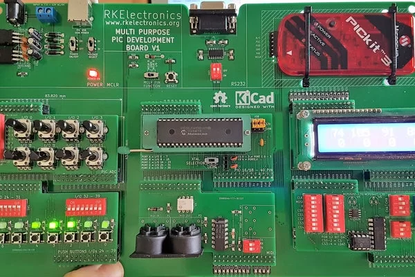
The first PCB is a main back plane board which hosts the power supply, MCLR reset circuit, RS232 and PICKIT programmer pin-header. This board serves as an interconnecting board which holds up to six daughter boards.
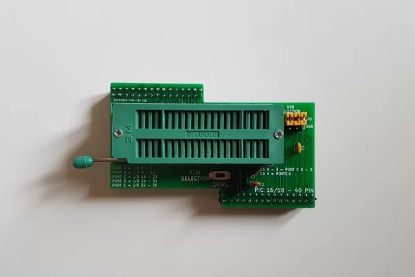
The second PCB board type is the daughter board component. A standardised PCB design and footprint is used to create a PCB board design which can be added and removed from the main board as desired. The purpose of the daughter board is host either a microcontroller or peripheral circuit for example, a Digital to Analogue Converter (DAC).
The design intent is to create daughter boards as required. This project therefore is ongoing.
As part of this project I have designed a number of basic daughter board designs that are available for Gerber / Project file download.
For details regarding specific daughter boards please see project document: PIC Controller Development Board – Daughter Board Catalogue, document ref: RKD3, made available with this document location or via my website at; www.rkelectronics.org/picdev
The daughter boards connect to the main board via two 2 x 30 2.54mm pitch pin headers. This allows daughter boards to be created either via a PCB fabrication house or by hand using Vero board.
Attachments
- Project Documentation – Main Board – RKD2.pdfDownload
- Project Documentation – Daughter Board Catalogue – RKD3.pdfDownload
Step 1: Daughter Boards
The main board and daughter board interconnect include the following busses;
1. 43 dedicated I/O lines for either analogue or digital,
2. VDD and GND power supply,
3. 5 dedicated SPI Chip Select (CS) lines,
4. SPI Buss for MOSI, MISO and CLK lines,
5. I²C shared as part of the SPI buss,
6. Dedicated TX and RX lines for RS232, RS485 and MIDI,
7. Dedicated D+ and D- lines for USB data,
8. Dedicated PIC programming lines, MCLR, PGD and PGC.
Due to the nature of SPI chip select lines, these lines are shared with various I/O lines. The sharing of which I/O line depends on the microcontroller daughter board used. It is intended that the connection of the CS lines to the microcontroller will be done on the daughter board. For example, for the PIC16/18 40 Pin USB daughter board for PIC18F4550 the CS lines share I/O pins 16, 17, 18, 19 and 32, which equates to PIC pins Port C0, C1, C2, C3 and E0. For this reason it is required for all peripheral boards using SPI to include a switch or breaker method to disconnect unused or other utilised CS lines.
Due to the nature of the RS232 TX and RX and USB D+ and D- lines, these lines are also shared with various other I/O lines. For this reason it is required for all peripheral boards using RS232, RS485 or USB to include a switch or breaker method to disconnect unused or other utilised TX, RX, D+ and D- lines.
The I/O lines are routed to various microcontroller pins, which pins are detailed within the daughter board schematic or the PCB silkscreen. Usually ports are routed to;
1. Port A = I/O lines 0 – 7,
2. Port B = I/O lines 8 – 15,
3. Port C = I/O lines 16 – 23,
4. Port D = I/O lines 24 – 31,
5. Port E = I/O lines 32 – 35,
Other PIC types such as dsPIC30/33 and 24 series will use different wiring arrangements.
Step 2: Gerber Files
This page contains the Gerber files required to manufacture the Main Board and Daughter Boards created so far. The list is as follows;
1. Main Board,
2. Main Board to 2nd Main Board connection,
3. dsPIC30F 28 Pin [Type A]
4. dsPIC30F 28 Pin [Type B]
5. dsPIC30F 28 Pin [Type C]
6. dsPIC30F 40 Pin [Type A]
7. dsPIC30F 40 Pin [Type B]
8. LEDs for I/O 0 – 39
9. MCP3208 [Type A]
10. MCP3208 [Type B]
11. PIC16-18 [8-14-20Pin][non USB]
12. PIC16-18[28Pin][non USB]
13. PIC16-18[40Pin][non USB]
14. PIC16-18[8-14-20Pin][USB]
15. PIC16-18[28Pin][USB]
16. PIC16-18[40Pin][USB]
17. Switches
18. ULN2003
19. Seven Segment
20. 12 Bit DAC
21. MIDI
22. PIC ADC
23. Push Buttons [Type A]
24. Push Buttons [Type B]
25. 16 x 2 Alphanumeric LCD Display
26. dsPIC30F [18 Pin]
27. Pin Header Breakouts
Attachments
- Main Board.zipDownload
- Module – 7 Segment.zipDownload
- Module – 12 Bit DAC.zipDownload
- Module – Board-To-Board Expansion.zipDownload
- Module – Breakouts.zipDownload
- Module – dsPIC30F 18Pin.zipDownload
- Module – dsPIC30F 28 Pin [A].zipDownload
- Module – dsPIC30F 28 Pin [B].zipDownload
- Module – dsPIC30F 28 Pin [C].zipDownload
- Module – dsPIC30F 40Pin [B].zipDownload
- Module – dsPIC30F-40Pin-A.zipDownload
- Module – LCD.zipDownload
- Module – LEDs.zipDownload
- Module – MCP3208 Type 2.zipDownload
- Module – MCP3208.zipDownload
- Module – MIDI.zipDownload
- Module – PIC ADC.zipDownload
- Module – PIC16-18 [8-14-20][nonusb].zipDownload
- Module – PIC16-18 [28][nonusb].zipDownload
- Module – PIC16-18 [40][nonusb].zipDownload
- Module – PIC16-18[8-14-20][USB].zipDownload
- Module – PIC16-18[28][USB].zipDownload
- Module – PIC16-18[40][USB].zipDownload
- Module – Push Buttons 1.zipDownload
- Module – Push Buttons2.zipDownload
- Module – Switches.zipDownload
- Module – ULN2003.zipDownload
Step 3: KiCAD Library Files
This bit here is for the KiCAD component library and footprint for the daughter board. You will need to add the edge cuts lines around the footprint before exporting your own gerber files.
Hope you enjoy this project!
my website for more projects is at
Attachments
Source: PIC Microcontroller Development Board System
- What is the overall design approach of the development system?
It uses a two-PCB design: a main backplane board and removable standardized daughter boards. - How do daughter boards connect to the main board?
Via two 2 x 30 2.54mm pitch pin headers. - How many dedicated I/O lines are available?
There are 43 dedicated I/O lines for analogue or digital use. - Does the system support SPI and how are CS lines handled?
Yes; there is an SPI bus with MOSI, MISO, CLK and five chip select lines which are shared with I/O lines and require switching on peripheral boards. - Are UART and USB lines shared with other I/O?
Yes; TX/RX and USB D+ and D- lines are shared with other I/O and peripheral boards must include switches or breakers to disconnect unused or conflicting lines. - What PIC ports map to I/O lines on typical daughter boards?
Typically Port A = I/O 0–7, Port B = I/O 8–15, Port C = I/O 16–23, Port D = I/O 24–31, Port E = I/O 32–35. - Are Gerber files available for modules and boards?
Yes; Gerber files are provided for the main board and numerous daughter and peripheral modules listed in the project. - Does the project provide KiCAD libraries?
Yes; KiCAD component library and footprints are available and require adding edge cuts before exporting Gerbers. - Can the daughter boards host both microcontrollers and peripherals?
Yes; daughter boards can host either a microcontroller or peripheral circuits such as DACs. - Is the project intended to be expandable and ongoing?
Yes; the design intent is to create daughter boards as required and the project is ongoing.