Summary of Mastering PIC 24F Series: A Comprehensive Guide with MPLAB and Proteus
This paper demonstrates using the PIC24FJ128GA010 microcontroller for ports, timers/interrupts, PWM, and peripheral interfacing, with development in MPLAB and simulation in Proteus. It details port initialization, timer1-based delays and interrupts, PWM generation via Output Compare Modules, and tools/workflow for creating and simulating hex files.
Parts used in the PIC24FJ128GA010 Project:
- PIC24FJ128GA010 microcontroller (100-pin)
- 16 MHz crystal oscillator
- Digital oscilloscope (virtual in Proteus)
- Push buttons (connected to RA1 and RA2 for PWM control)
- Proteus VSM simulation software
- MPLAB IDE (version 8.10) with C30 compiler
- Timer modules (internal to PIC24FJ128GA010)
- Output Compare Modules OC1, OC2, OC3 (internal to PIC24FJ128GA010)
- Ports A and B (I/O pins of the microcontroller)
Introduction
The field of embedded systems plays a crucial role in modern society, with a myriad of applications across various sectors such as telecommunication, medical devices, industrial control, and more (Miha & Mihael, 2008). Microcontrollers form the backbone of these embedded systems, capable of executing complex operations based on hundreds of thousands of transistors. Initially, microprocessors lacked built-in peripherals like memory, I/O lines, and timers (Yousif, 2012). The introduction of integrated circuits (ICs) marked a significant development, combining processors and peripherals into a single device known as a microcontroller (N. Barsoum, 2010).
Peripheral Interface Controllers (PICs), developed by Microchip Technology, Inc., emerged as cost-effective units featuring a built-in central processing unit (CPU), I/O functions, memory, and timers (S.H. LEE et al., 2004). Microchip quickly became a leading supplier of 8-bit controllers, introducing various families, including 10xxx, 12xxx, 14xxx, 16xxx, 17xxx, and 18xxx. Among the 8-bit microcontrollers, the PIC18xxx series, especially the PIC18F, showcased superior performance (M.A. Mazidi et al., 2008).
In response to technological advancements and the demand for high performance, Microchip introduced 16-bit microcontroller families like 24F, 24H, dsPIC30F, and dsPIC33F. The PIC 24F series, in particular, stands out by delivering enhanced performance compared to the PIC18xxx series with minimal cost implications (D. Schneider, 2006). This research focuses on the PIC24FJ128GA010 microcontroller, demonstrating its functionality through algorithm development, hex file generation using MPLAB Microchip development tools, and simulation in Proteus Professional.
The paper is structured as follows: Section 2 provides a detailed discussion of the PIC24FJ128GA010 microcontroller. Section 3 covers the software tools used, while Section 4 initializes the ports. Section 5 elaborates on timers and interrupts, while Section 6 addresses PWM. Section 7 explores the interfacing of LCD and keypad with the microcontroller’s I/O ports. Section 8 delves into asynchronous serial communication using UART. Finally, Section 9 summarizes the conclusions drawn from the research work.
The PIC24FJ128GA010, part of the CMOS family, boasts low power consumption attributed to its power management modes, namely sleep, idle, and alternate clock modes. Operating within a voltage range of 2.0 V to 3.6 V, this microcontroller is a versatile 100-pin device featuring a modified Reduced Instruction Set Computer (RISC) architecture. It can function with a crystal oscillator of up to 32MHz, achieving a speed of 16 Mega Instructions Per Second (MIPS) (PIC Datasheet, 2006). Optimized for C compiler usage, the controller employs a dynamic addressing mode in its instruction set mechanism (S. Aslam, 2015). With a 16-bit wide data memory bus and a 24-bit wide program memory bus, the PIC24FJ128GA010 is equipped for a variety of applications.
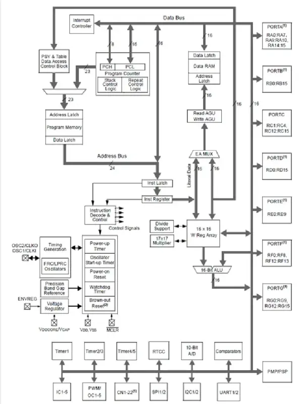
It possesses 128 kilobytes (KB) of program memory, 8KB of RAM data memory, and incorporates five 16-bit timers/counters with a programmable prescaler. Additionally, it offers seven communication modules, including I2C, UARTs, SPIs, and a Parallel Master Port (PMP) (L.D. Jasio, 2007). The peripheral characteristics of the PIC24F family are outlined in Table 1 (PIC Datasheet, 2006).
A microcontroller’s port comprises pins that serve as the physical link between the Central Processing Unit (CPU) and the external environment, allowing the microcontroller to manage or observe other systems (N.Matic, 2003). The PIC24FJ128GA010 model encompasses six ports labeled A, B, C, D, E, F, and G, all of which can be configured as inputs or outputs based on the microcontroller’s application requirements. Notably, Port B pins, by default, are multiplexed with analog inputs, necessitating a connection to digital inputs for use as outputs (L.D.Jasio, 2007).
To designate ports as inputs or outputs and link Port B pins to digital inputs, control registers TRISX and AD1PCFG are employed, with X denoting the specific port. Upon reset, all I/O pins default to input configuration. Therefore, initializing Port B as an output requires sending 0x0000 to TRISX, while connecting I/O pins to digital inputs involves sending 0xFFFF to AD1PCFG. In this context, Port A and Port B are initialized as outputs, and Port B pins are linked to digital inputs to enable external devices to read information from Port B pins. Subsequently, toggling of the first four pins of both ports is executed.
The program is developed in MPLAB using the command sequence depicted in Figure 4. The initial step involves including the header file of the PIC24FJ128GA010 model, serving as a pseudo-instruction for the pre-processor to access device-related information. In the main function, control registers are initialized, and the specified data is transmitted to the output through both ports. Simulations of PORTS A and B are conducted in Proteus, with the results illustrated in Figure 5.
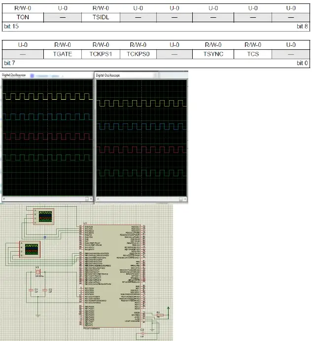
Figure 5(a) displays the circuit diagram implementation in Proteus, while Figure 5(b) illustrates the toggling of the initial four pins on both ports observed on a digital oscilloscope, utilizing the VSM feature of Proteus.
Timers represent fundamental peripherals in every microcontroller, offering a range of functionalities such as timers, counters, internal and external interrupts, and A/D event triggers (Z. Milivojević & D. Šaponjić, 2008). The PIC24FJ128GA010 microcontroller is equipped with five 16-bit timers, and the combination of timer 2/3 and timer 2/4 allows the creation of a 32-bit timer or counter. The operational modes and various features provided by timers are activated through the corresponding bits in the TXCON control registers (PIC Datasheet, 2006).
This section focuses on the application of timer 1 for generating delays, detailing its functionality, development, and simulation. Two crucial special function registers, TMR1 (a 16-bit counter) and PR1 (utilized for producing periodic resets, often employed for interrupt purposes), are employed in timer 1 applications (L.D.Jasio, 2007). Additionally, T1CON, a 16-bit control register illustrated in Figure 6 (L.D.Jasio, 2007), plays a key role in configuring and controlling timer 1 operations.
The timer1 control register bits are precisely defined as follows: The TON bit activates timer 1, TSIDL specifies behavior in idle mode, TGATE and TSYNC bits are utilized when a timer clock other than the MCU internal clock is employed. The TCKPS bits allow the selection of a prescaler level to determine the incrementation of TMR1 after a specified number of MCU internal clock cycles. The TCS bit, set to 0 when using the MCU main clock source, designates the clock source.
For the purpose of employing timer 1 for delay, T1CON should be configured with the TON bit set to 1. The TSIDL bit is irrelevant for this purpose, and TGATE, TSYNC, and TCS are also set to 0, assuming the MCU internal clock of 32MHz is used as the clock source. TCS bits are set to (11) for the maximum prescaler of 1:256, given the options of 1:1, 1:8, 1:16, 1:256. The initialization of T1CON involves assigning the value 0x8030 to it. To achieve a specific delay time, Equation (1) is employed.
Here, T_delay represents the delay time, FOSC is the frequency of the MCU oscillator, and Delay is the value of clocks required for the particular delay. To observe the delay in simulations, the first four pins of PORTA are toggled with an ON time of 256ms and an OFF time of 160ms. Delays of 16000 and 10000 are calculated for time delays of 256ms and 160ms, respectively.
Interrupts are abrupt occurrences within the continuous execution flow of a series of commands (Z. Milivojević & D. Šaponjić, 2008). The PIC 24F family incorporates a dynamic interrupt system capable of managing 118 distinct interrupt sources, categorized as internal and external interrupts. Internal interrupt sources encompass timers, A/D converter, Analog Compare Module, and others, while external interrupt sources include pins for level trigger detection, pins connected to the change notification module, UARTS, and more. Each interrupt source is associated with a unique piece of code known as the Interrupt Service Routine (ISR). The syntax for the ISR is provided below:
“`C
Void _ISR _X1Interrupt(void) {
// ISR Code here
}
“`
Here, ‘X’ signifies the interrupt source. Each interrupt source is associated with five control bits: Interrupt Enable (_IE), Interrupt Flag (_IF), and three bits of Interrupt Priority Level (IPL0-IPL2). The IE bit must be set to 1 to enable the interrupt, the IF bit must be cleared at the end of the ISR to prevent immediate re-calling of the same ISR, and the IP bits set the priority of the interrupt source. Interrupt sources can have a maximum of 7 priority levels to address simultaneous occurrence issues by responding to the interrupt with a higher priority level.
An additional crucial bit is _NSTDIS, which prevents interrupting a low priority level interrupt with a high priority level interrupt. This bit must be set to 1. In this section, Timer 1 is explained as an internal interrupt source by setting a pin of PORTA to high for 100 ms. After that, an interrupt will be generated, and in the ISR, the PORTA pin will be set to low, and the PORTB pin will be set to high immediately for 50 ms. The required number of clock pulses to generate 160 ms is calculated using equation (1), and that value is assigned to the PR1 register of Timer 1. The delay of 50 ms in the ISR is generated using Timer 2. The application of Timer 1 as an internal interrupt source is developed in MPLAB by following the command sequence illustrated in Figure 9.
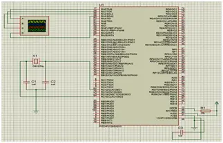
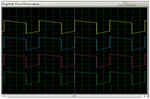
Figure 8. Simulation of Toggling PORTA with Delay
The depicted diagram illustrates the circuit configuration where PORTA and PORTB pins are linked to Channel A and Channel B of the digital oscilloscope, respectively. The simulation distinctly indicates that the initial PORTA pin remains in a high state for 100 ms. Following the occurrence of an interrupt, the PORTA pin transitions to a low state, while the PORTB pin shifts to a high state and maintains this state for the subsequent 50 ms. This sequence then repeats in a continuous manner.
PWM, a sophisticated method of delivering varying amounts of electrical power between fully ON and fully OFF, stands in contrast to conventional power switches that provide only full power when turned on. This relatively recent electronic power switch technology is instrumental in achieving PWM (A.K. Dewangan et al., 2012). In the PIC24FJ128GA010 microcontroller, the Output Compare Module (OCM) is employed to generate PWM, utilizing three pins: OC1, OC2, and OC3. OCM offers various operational modes, including Single Compare Match Module, Double Compare Match Mode Generating, and Simple PWM. Initialization of OCM involves configuring the OCXCON control register, with the first three bits (OCXCON<2:0>) set to (110)₂ for PWM generation.
To determine the PWM frequency, the number of cycles required to produce the PWM period is written to the period register of the selected timer, calculated using Equation (2) (PIC Datasheet, 2006), where PWM frequency = 1/[PWM Period] and TCY = 2/FOSC. The duty cycle of PWM is established by writing its value in the OCXRS register. Initially, the duty cycle’s value is written to the OCXR register, which subsequently becomes a Read-Only duty cycle register after initializing the OCXCON control register for simple PWM generation (PIC Datasheet, 2006).
In this research project, PWM with a frequency of 488 Hz is generated using a 16 MHz crystal oscillator. The calculated value of clocks for the period register, using Equation (2), is (7FFA)₁₆, and the initial value of PWM written to the OCXR register is (0F)₁₆. Timer 2 is employed to generate interrupts at a frequency of 488 Hz. In the Proteus simulation, two push buttons are connected to pins RA1 and RA2 to increase and decrease the PWM duty cycle, respectively.
- What development tools are used to create and simulate applications for the PIC24FJ128GA010?
The research uses MPLAB IDE (version 8.10) with the C30 compiler to create hex files and Proteus VSM to simulate microcontroller applications. - How are ports initialized for digital output on the PIC24FJ128GA010?
Ports are configured by writing to TRISX to set direction and to AD1PCFG to connect Port B pins to digital inputs; sending 0x0000 to TRISX sets a port as output and 0xFFFF to AD1PCFG connects I/O pins to digital inputs. - Can Timer1 be used to generate delays on the PIC24FJ128GA010?
Yes; Timer1 uses TMR1 and PR1 with T1CON configured (example value 0x8030) and equation (1) to calculate clock counts for desired delays such as 256 ms and 160 ms. - How are interrupts implemented for Timer1 in this project?
Timer1 is set as an internal interrupt source with an ISR using the Void _ISR _X1Interrupt(void) syntax; the IE bit enables the interrupt and the IF bit must be cleared in the ISR. - What behavior is produced when Timer1 interrupt occurs in the simulation?
PORTA pin remains high for 100 ms, then an interrupt sets PORTA low and PORTB high for 50 ms, repeating continuously as shown in the Proteus simulation. - How is PWM generated on the PIC24FJ128GA010?
PWM is generated using the Output Compare Module (OCM) by setting OCXCON bits to 110₂ for PWM mode, writing period value to the timer period register and duty cycle to OCXRS/OCXR. - What PWM frequency and settings were used in the project example?
A 488 Hz PWM was generated using a 16 MHz crystal; the period register value was (7FFA)₁₆ and initial OCXR duty value was (0F)₁₆, with Timer2 generating interrupts at 488 Hz. - How is PWM duty cycle adjusted in the Proteus simulation?
Two push buttons connected to RA1 and RA2 are used to increase and decrease the PWM duty cycle in the Proteus simulation.