Summary of Hands-On Microcontroller Projects: BK300 Development Board Featuring PIC16F887 Chip Lab
Summary (under 100 words): The article describes a low-cost, project-based microcontroller laboratory using the BK300 development board and PIC16F887. It outlines hardware and software setups (PICKit3, mikroC PRO for PIC, Proteus, PICKit3 debugger), step-by-step programming and simulation procedures, and four hands-on experiments: LED on/off, LCD display, four-digit seven-segment timer, and LM35 temperature sensor with LCD. The work emphasizes bridging theory and practice in embedded systems education and compares the BK300/PIC16F887 solution favorably to similar, costlier setups.
Parts used in the BK300 PIC16F887 Project:
- BK300 PIC development board
- PIC16F887 microcontroller chip
- PICKit3 programmer
- USB cable / USB extension cord
- Personal computer (PC)
- ZIF 40-pin socket (on BK300 board)
- Jumper selector cable
- LEDs (8 for parallel I/O experiment)
- 16x2 LCD module
- Four-digit multiplexed seven-segment display
- LM35 temperature sensor
- Assorted electronic components (wires, resistors, switches SW1/SW2)
- Proteus 8.0 (VSM) software
- mikroC PRO for PIC compiler
- PICKit3 software debugger
1. INTRODUCTION
The study of microcontroller systems is experiencing a global surge across various fields within science, engineering, and technology departments of universities and polytechnics [1-2]. The utilization of microcontroller chips to oversee embedded system functions is witnessing rapid growth in daily technological design practices within colleges and research institutes
A microcontroller represents an entire computer consolidated onto a single chip, encompassing all functionalities present in a microprocessor. For example, microcontrollers serve as control units in automobiles and act as focal point controllers in camera systems. Specifically tailored for such applications, they boast extensive on-chip resources including built-in ROM, RAM, I/O ports, Serial and Parallel I/O ports, Timers, Counters, Interrupt controllers, Analog-to-Digital Converters, and Clock circuits. Their robust digital processing capabilities significantly enhance application effectiveness owing to the degree of control and programmability they offer.
Teaching a microcontroller system course to departments like computer engineering, telecommunication engineering, electrical and electronics engineering, and computer science students using traditional methods proves to be ineffective and inadequate if it lacks hands-on laboratory sessions [4]. Understanding embedded systems development, microcontroller system interconnections, and configurations is crucial for practical learning. Embedded systems are extensively utilized across various fields, increasing the demand for skilled professionals in this domain. Unfortunately, teaching methods and practical training in embedded systems are falling behind [5]. A major challenge in teaching microcontroller system courses is bridging the gap between theoretical knowledge and practical experiences for students [6].
Descriptions of experiments in microcontroller system teaching are continuously reviewed and enhanced, adapting to changes in microcontroller chip architectures [7]. Typically, students gain deeper knowledge and skills when actively participating in both practical and theoretical learning. Passively engaged students in lecture-based courses face substantial difficulty in grasping embedded system design and microcontroller programming concepts [8]. Therefore, structuring microcontroller system courses to offer not only theoretical understanding but also substantial practical exposure is essential. Initiating early hands-on laboratory experiments in microcontroller systems during students’ academic studies ensures a more effective comprehension of the course. This method supplements learners’ theoretical knowledge, promotes modern teaching practices, fosters international project collaborations, and encourages cooperative learning processes [9-11].
A structured approach to hands-on laboratory work aims to instill confidence, enhance skills, promote self-reliance, and foster creative thinking in students regarding embedded system design and development using microcontroller chips [12]. The criteria for selecting a microcontroller for an embedded system encompass various factors:
– Fulfilling computing requirements cost-effectively.
– System operation speed.
– Packaging of the system.
– System power consumption.
– On-chip memory capacity (RAM and ROM).
– Number of I/O pins and on-chip timers.
– Availability of software development tools like compilers, assemblers, and debuggers [13-15].
2. RELATED WORK
Numerous pieces of literature delve into the creation and advancement of project-based microcontroller and embedded systems in laboratory settings. In [17], authors proposed a project-centered course in embedded systems design utilizing a reconfigurable SoC platform. This initiative addressed laboratory challenges linked with embedded systems, showcasing diverse applications from controlling small unmanned aerial vehicles to image processing. Students gained practical experience in configuring peripherals without prior knowledge of embedded system circuit design and simulation, making this course an elective within the curriculum.
In another study outlined in [3], the focus rested on crafting and evolving a project-oriented embedded system laboratory employing LPC1768. This approach aids students in comprehending the fundamental components of embedded systems through progressive hardware design, covered within a single third-semester laboratory course.
This research does not encompass microcontroller concepts and embedded circuit simulation. It showcases a detailed demonstration of a low-cost embedded system laboratory designed and developed using the TI MSP430 [18]. Notably, the experiments conducted here include both hardware descriptions and software development in each hands-on lab. However, the drawback of this research proposal lies in its personalized design and development for training purposes, making it challenging for others to adopt this system for their own research and hands-on lab experiments in embedded system development within their regions.
Another research effort on embedded systems home experimentation by [19] introduces an alternative approach to embedded system development laboratory exercises. This approach involves expanding the number of workstations in the lab, utilizing simulators instead of real embedded hardware, and facilitating distance learning of hands-on lab exercises. Additionally, authors in [20] present a progression from microcontroller system concepts to printed board implementation. Their work involves utilizing the microcontroller system for experiments involving analog signal to digital signal conversion, starting from simulated circuitry to designing the printed board layout. This process was developed and tested in both open loop and closed loop systems to enhance students’ skills in microcontroller systems.
Most of the aforementioned reviews focus on project-based design and development of embedded systems. However, this paper aims to simplify the complexities in embedded system design, ranging from microcontroller project-based circuit design, circuit simulation, and development concepts. The goal is to provide comprehensive hands-on lab exercises and enhance learners’ skills from basic embedded system design to more advanced robotic systems.
3. Hardware, Software System Description And Their Architecture
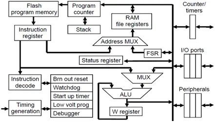
HARDWARE SYSTEM DESCRIPTION AND ITS ARCHITECTURE
This paper discusses the hardware components utilized for programming the microcontroller chip, which include the PICKit3 programmer, BK300 PIC development board, PIC16F887 chip, USB extension cord, a personal computer system, and various electronic components. The setup of the hardware system followed these steps:
– Connecting the BK300 PIC development board to PCs via a USB cable interface,
– Attaching the PICKit3 programmer to the development board using a jumper selector cable,
– Establishing the connection of the PICKit3 programmer to PCs using a USB cable,
– Placing the PIC16F887 microcontroller chip onto the 40-pin ZIP socket located on the BK300 PIC development board and securing it by pulling down the notch to firmly hold the chip,
– Finally, powering the board by pressing the switch button SW1.
3.2: SOFTWARE SYSTEM DESCRIPTION AND THEIR ARCHITECTURE
The programming code and simulation in this project utilize the mikroC Pro for PIC software, Proteus 8.0 (VSM), and the PICKit3 software debugger as the compiler. This paper outlines the software’s usage, detailing the stages of program code compilation and development. These aspects are elaborated upon in the block diagram and flowchart illustrated in figures 3 and 4, respectively.
3.3 DETAILS OF PROGRAMMING PROCEDURE AND SIMULATION USINGMIKROC PRO PIC SOFTWARE
This paper includes the steps within the programming process and provides an overview of the simulation programs involved.
Stage One: System Configuration
This entails initiating a New Project File, composing the source code, and compiling it into a .Hex file using the mikroC PRO for PIC software (Text Editor). This phase involves specific configuration settings:
– Defining the project name and an optional description.
– Specifying the target device.
– Setting device flags (config word).
– Configuring the device clock.
– Compiling a list of project source files with their respective paths, including header files (*.h), binary files (*.mcl), image files, and other relevant files.
To complete the initial configuration in this first stage, follow these steps:
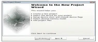
Step 1: Access the main menu bar and navigate to Project › New Project › then click on the Next button. Alternatively, you can click on the New Project Icon found in the Project Toolbar.
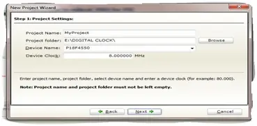
Step 2 involves performing the following tasks within the project settings:
Choose the Project Name, Project folder, the device name, and the device clock in MHz from their respective drop-down lists. For example, select (LED Blink, C:\Users\Desktop\Computer Lab work, P16F887, and 4.000000MHz) and proceed by clicking on the Next button.
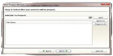
Step 3: Select the file you want to add to the file and click on Next button.
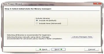
Step 4: Select the initial state for library manager. Hint; select all by default is recommended for the beginners.
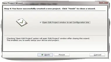
Step 5: Validate the configuration settings by selecting the “Edit Projects” window button, then proceed to click the “Finish” button to successfully generate the project file and folder.
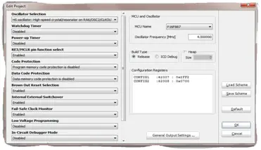
3.3.2 STAGE TWO: SOFTWARE DEVELOPMENT
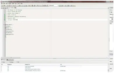
This marks the second phase within the programming process and simulation program. It involves transitioning from designing the source code to generating object code (.hex file) for hardware programming using software compiler or assembler tools. Figure 12 illustrates the compiler interface (mikroC code editor), which includes the main menu, toolbar, code folding, code assistance, parameter assistance, and more. This stage is aimed at achieving…
3.3.3 Stage Three: Software Design and Implementation
This represents the final phase where both the hardware system and software program are implemented to achieve a fully operational embedded system. The development board is linked to the PICKit3 programmer, which in turn interfaces with a PC (Terminal Emulator, Monitor ROM, and Programmed Code). Below are the step-by-step procedures for executing software design implementation on the microcontroller chip.
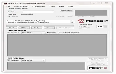
• a. Connect the PICKit 3 programmer to the PC. Upon powering up and displaying the active light, proceed to open the installed PICKit 3 programmer software.
• b. Within the main menu of the PICKit 3 software, navigate to Device family and select the MCU architecture (Midrange).
• c. Under Device Configuration, choose the specific MCU (such as PIC16F887) where the .hex file is intended for download.
• d. Click on File, then select Import to import the object code (.Hex file).
• e. Access the Programmer option on the menu bar and choose Write Device to erase the MCU’s content and ultimately deploy the .hex code onto the device for programming.
4. DESCRIPTION OF CIRCUIT SIMULATION EXPERIMENTSAND INDIVIDUAL HAND-ON LABORATORY EXERCISES
This paper presents four distinct experiments utilizing available hardware and software tools. For each experiment, a circuit simulation diagram is created using Proteus 8.0 software, and hands-on laboratory experiments are conducted using the hardware system outlined in section 3.1. All components are visually integrated within each experiment. The experiments include ON/OFF LED display, LCD module message display, Seven-segment count-down timer, and temperature sensor with LCD module interface. Through these showcased experiments, this paper contributes to enhancing students’ theoretical understanding in learning microcontroller systems as a course and refining their practical skills in embedded system design and interfacing microcontroller chips with various electronic components. This practical exposure aids students in configuring these systems for laboratory research, industry applications, and global development [16].
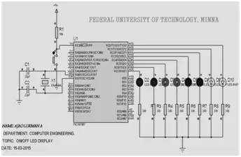
EXPERIMENT 1: PARALLEL I/O ON/OFF LED INTERFACING
In the initial experiment involving LED interfacing for on/off operations, eight LEDs were arranged in parallel and connected to the PIC16F887 through Port B (RB0-RB7), using pins 33-40 on the microcontroller chip. The following steps outline the process of programming the PIC16F887 chip using both hardware and software tools to execute and showcase the experiments:
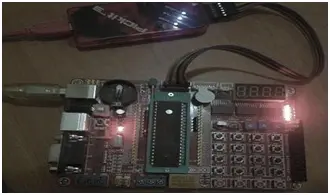
1. Establish a connection between the PC and the BK300 PIC development board using a USB cable for power supply.
2. Connect the PICKit3 programmer to the ICSP port J7.
3. Connect the PC and the PICKit3 programmer via a USB cable for power supply.
4. Activate the power switch (SW2) to power up the board.
5. Position the PIC 16F887 chip onto the 40-pin ZIF socket of the board. If it’s already in place, proceed to the next step.
6. Launch the MikroC PRO for PIC compiler on your PC. Create a new project and folder named ‘LED Blink’. Select PIC 16F887 as the target device and set the clock frequency to 4MHz. Write the code in the code editor window and click ‘build’ to compile the project (.HEX) code.
7. Open the PICKit 3 programmer GUI on the PC. Choose Midrange under device family, then click on ‘Import Hex’ under File and navigate to the project folder. Load the project (.HEX) code. Click ‘Write’ to erase and program your chip.
8. Observe the simultaneous on/off blinking of the 8 LEDs on the board at precise intervals as per the instruction code, displaying continuous operation.
4.1. EXPERIMENT 1: PARALLEL I/O ON/OFF LED INTERFACING
In the initial experiment involving the on/off LED Interfacing, a configuration of eight LEDs was employed and set up in parallel before interfacing with the PIC16F887 through Port B (RB0-RB7), which utilizes pins 33-40 of the microcontroller chip. The following steps outline the process of programming the PIC16F887 chip using both hardware and software tools to execute the experiments and demonstrate the functionality:
• Establish a connection between the PC and the BK300 PIC development board using a USB cable to power the system.
• Connect the PICKit3 programmer to the ICSP port J7.
• Use another USB cable to connect the PICKit3 programmer to the PC for power.
• Depress the power switch at SW2 to activate the board.
• Place the PIC 16F887 chip onto the 40-pin ZIF socket on the board. If the chip is already in place, proceed to the subsequent step.
• Launch the MikroC PRO for PIC compiler on your PC. Generate a new project and designate a folder named ‘LED Blink’. Select PIC 16F887 as the target device and set the clock frequency to 4MHz. Compose the code within the code editor window and click ‘build’ to compile the project into (.HEX) code.
• Start the PICKit 3 programmer GUI on the PC. Choose ‘Midrange’ in the device family selection. Under ‘File’, select ‘Import Hex’ and navigate to the project folder. Load the project (.HEX) code. Click on ‘Write’ to erase and program your chip.
• Observe the synchronized blinking of 8 LEDs on the board, alternating between ON and OFF states at precise intervals, following the instruction code, displaying continuous functionality.
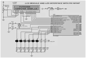
4.2 EXPERIMENT 2: LCD MODULE INTERFACING
In Experiment 2, the LCD and LED serve as output devices connected to Port A and Port C of the controller system, respectively. To program the chip for this experiment, follow the same steps outlined in Experiment 1, spanning from steps i to vii. Only modify your code at step (vi) and compile it to generate the .Hex file. This process can be used to program the PIC16F887 chip for subsequent experiments, namely Experiments 3 and 4 detailed in this paper.
Upon execution, observe the continuous display of the message “FUTMINNA” and “COMPUTER ENGR. LAB” on the 16×2 LCD module. This message persists until any external modification or power failure occurs, while the eight LEDs glow simultaneously.

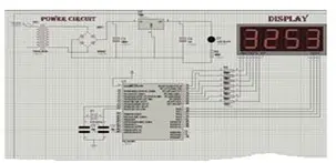
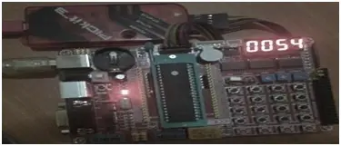
4.3 EXPERIMENT 3: FOUR-DIGITS MULTIPLEXED SEVEN-SEGMENTDISPLAY INTERFACING
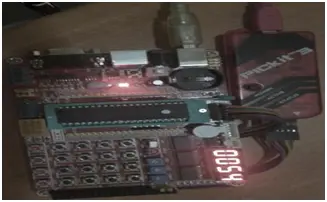
Within this experiment, the PIC16F887 chip interfaces with a four-digit multiplexed seven-segment display via Port B. The primary task involves executing a basic operation known as a count-down timer (ranging from 0 to 99) at a predefined interval.
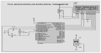
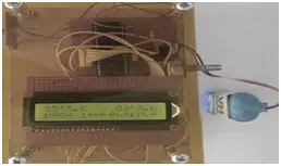
4.4 EXPERIMENT 4: TEMPERATURE SENSOR AND LCD INTERFACE WITHPIC16F887
Experiment 4 involves utilizing a digital thermometer (LM35) to gauge the room temperature. The experiment employs an LCD and an LM35 temperature sensor, connected to Port B and Port A pin 4, respectively. The measured temperature value in Celsius (°C) is converted to its corresponding Fahrenheit (°F) value, and both readings are showcased on the LCD screen.
5. COMPARATIVE STUDY WITH SIMILAR WORKS INLITERATURE
A comparison was conducted between the creation of a project-based microcontroller system laboratory utilizing the BK300 development board featuring the PIC16F887 chip and similar works documented in the literature. The comparison considered various aspects such as features, functions, cost, and architecture in the development of low-cost embedded systems, including works by Aruna et al. (2013), Naveen et al. (2013), Daniel et al. (2015), as well as the concept of microcontroller system development highlighted in works by Wilfried et al. (2003) and Edgard et al. (2010).
Through this comparative analysis, it was determined that the utilization of the BK300 development board and the PIC16F887 chip exhibits superior advantages over other existing similar works, as detailed in Table I.
Table I: Comparison of the BK300 development board and PIC16F887 with adopted works in literature.
| S/N | Parameter of Comparison | Aruna et al., 2013, Naveen et al., 2013 and Daniel et al.,
2015. |
Project-based microcontroller system laboratory using Bk300 development
board with PIC16F887 chip |
| 1. | Described Features | This laboratory development board has limited features and support little applications as described in authors’ paper. | This has common features of most laboratory development board with additional structures like electronic clock experiment (using DS1302 Electronic Clock), buzzer (MCU sound, music play), 12864 LCD interface (characters display, image display and man-machine interface), infrared receiver interface, PS2
keyboard interface and ICSP simulation programming interface. |
| 2. | Functions | As described in the authors work (Aruna et al., 2013, Naveen et al., 2013), the boards are suitable to carried out some laboratory
experiments exercises based on their features but limited. |
This Bk300 development board laboratory tools has many features and support applications more than the existing boards in the Aruna et al., 2013, Naveen et al., 2013, and also as
mentioned in parameter 1 of the table I. |
| 3. | Cost | Board considered in these works are expensive than the proposed board in our contribution. As NXP LPC1768 is $49 and MSP430
LaunchPad and the development board is over $45. |
This tools is considered to be less expensive compared to the existing one ($33.69) |
| 4. | Microcontroller Architecture | In the authors work (Aruna et al., 2013, Naveen et al., 2013), the microcontroller used for programming are expensive, scarce and not generally accessible to the users compared to the BK300 board. Each pin has little functions compared to the
microchip PIC16F887. |
PIC16F887 is the microcontroller used for programming from microchip company. This chip is considered to be less expensive ($2.8), compact, and easy to study. It’s generally available in the market for the user consumption and applications. Each pin is configured to perform more than one function in the capacity of
applications. |
- What hardware is used to program the PIC16F887 in this project?
The project uses a BK300 PIC development board, a PIC16F887 chip, and a PICKit3 programmer connected to a PC via USB. - How is a new project configured in mikroC PRO for PIC?
Create New Project, set project name and folder, select target device and device clock, add source files, configure library manager, validate settings and finish. - Can the LEDs be controlled in parallel with the PIC16F887?
Yes; eight LEDs were interfaced in parallel to Port B (RB0-RB7) and programmed to blink on/off. - How is the compiled .hex file written to the microcontroller?
Open PICKit3 software, select device family Midrange and device PIC16F887, import the .hex file, then use Write Device to program the MCU. - What software tools are used for simulation and compilation?
Proteus 8.0 (VSM) is used for circuit simulation and mikroC PRO for PIC is used for code development and compilation; PICKit3 software is used for debugging/programming. - How is the LCD used in the experiments?
The 16x2 LCD is connected as an output device (e.g., to display FUTMINNA and COMPUTER ENGR. LAB) and interfaced to controller ports as described in the LCD experiment. - Does the project include a temperature sensing experiment?
Yes; Experiment 4 uses an LM35 temperature sensor connected to Port A pin 4 and displays Celsius and Fahrenheit on the LCD. - What does the seven-segment experiment demonstrate?
It demonstrates interfacing a four-digit multiplexed seven-segment display to implement a count-down timer using Port B. - What are the power-up steps for the BK300 board before programming?
Connect the BK300 board to PC via USB, attach PICKit3 to ICSP port and PC, place PIC16F887 in ZIF socket, then power the board using the SW1/SW2 switch.