Summary of 555 timer in different modes of operation with circuit diagram
This article details the operation of the 555 timer chip in monostable, astable, and bistable modes. It explains internal components like resistors, comparators, flip-flops, and transistors to define voltage references and output states. The text provides mathematical formulas for pulse duration in monostable mode and lists applications such as oscillators, time delays, and basic storage systems.
Parts used in the 555 Timer Project:
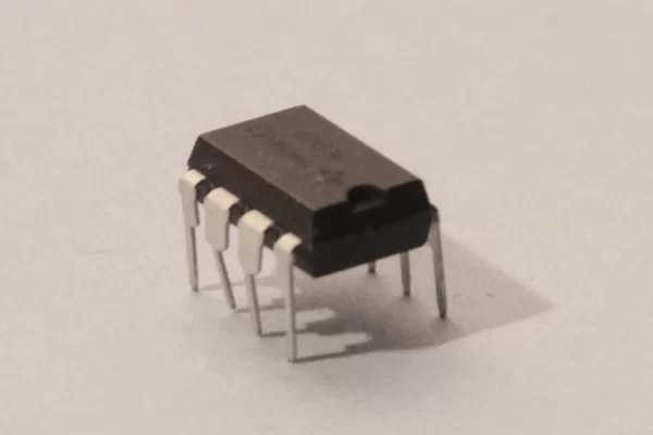
- 555 Timer Chip
- Resistors (including three 5kOhm internal resistors)
- Capacitors
- NPN Transistor
- PNP Transistor
- Comparators
- Flip Flop
- Output Stage Buffer
- LED Indicator
- Speaker
This tutorial provides sample circuits to set up a 555 timer in monostable, astable, and bistable modes as well as an in depth discussion of how the 555 timer works and how to choose components to use with it. The 555 timer is a chip that can be used to create pulses of various durations, to output a continuous pulse waveform of adjustable pulse width and frequency, and to toggle between high and low states in response to inputs. By wiring the 555 timer with resistors and capacitors in various ways, you can get it to operate in three different modes:
Monostable Mode is great for creating time delays. In this mode an external trigger causes the 555 timer to output a pulse of an adjustable duration. Jump straight to an example circuit for monostable mode here.
Astable Mode outputs an oscillating pulse signal/waveform. In this mode the output of the 555 timer is switching between high and low states at a tunable frequency and pulse width. Jump straight to an example circuit for astable mode here.
Bistable Mode causes the 555 timer to toggle its output between high and low states depending on the state of two inputs. Jump straight to an example circuit for bistable mode here.
Some applications that come to mind include:
– a steady clock/trigger to keep time in a circuit (astable mode)
– the core oscillator of an analog synthesizer, with the addition of some op amps and other components this pulse wave can be shaped into a triangle, saw, and even sine shapes
– a very basic chiptune style noise maker (see atari punk console)
– time delay for an incoming signal (monostable mode)
– very basic storage of input data/management of two button control system (bistable mode)
The 555 timer is flexible, cheap, and easy to find (you can even pick them up at Radioshack). It’s also a great starting point for audio projects because its output can be wired directly to a speaker.
Step 1: 555 Timer Pin Diagram
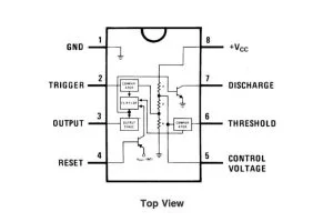
Fig 1 shows the pin connections to the 555 timer, it was take directly from the 555 timer datasheet. The power connections to the chip are through pins 1 (ground) and 8 (+Vcc). The positive supply voltage (+Vcc) should be between 5 and 15V.
The second image is a close up of the diagram depicting the internal functional components of the chip. This consists of a few different elements: resistors, transistors, comparators, a flip flop, and an output stage.
All three resistors diagrammed in fig 2 are 5kOhm (see image notes in fig 3). The purpose of these resistors is to set up a voltage divider between Vcc and ground. Since all resistors are the same value we know that the voltage at the junction between the resistors are 2/3Vcc and 1/3Vcc (see image notes in fig 2). These voltages are used as reference voltages for the comparators.
A comparator is a circuit which compares an input with a reference voltage and outputs a LOW or HIGH signal based on whether the input is a higher or lower voltage than the reference. The 555 timer uses several transistors to construct its comparators (see the image notes in fig 3), so in the simplified functional diagram in fig 2 they are represented by boxes labelled “comparator.” The comparator connected to pin 2 compares the “trigger” input to a reference voltage of 1/3Vcc and the comparator connected in pin 6 compares the “threshold” input to a reference voltage of 2/3Vcc from the voltage divider.
A flip flop is circuit that switches between two stable states based on the state of its inputs. The 555 flip flop outputs a high or low based on the states of the two comparators. When the trigger comparator is outputting a low signal (regardless of the state of the threshold comparator), the flip flop switches high, when both comparators are outputting a high signal, the flip flop switches low. The timing of a high pulse output from the flip flop can also be manually reset (the beginning of a pulse can be triggered) by pulsing the reset pin low.
The functional diagram in fig 2 also includes two transistors. The transistor attached to pin 7 is an NPN transistor. Since pin 7 is connected to the collector pin of the NPN transistor, this type of configuration is called open collector or open drain. This pin is usually connected to a capacitor and is used to discharge the capacitor each time the output pin goes low. The transistor attached to pin 4 is a PNP transistor. The purpose of this transistor is to buffer the reset pin, so the 555 does not source current from this pin and cause it to sag in voltage.
The output stage of the 555 timer is indicated in the image notes of fig 3. Its purpose is to act as a buffer between the 555 timer and any loads that may be attached to its output pin. The output stage supplies current to the output pin so that the other functional component of the 555 timer don’t have to.
Step 2: 555 Timer: Monostable Mode
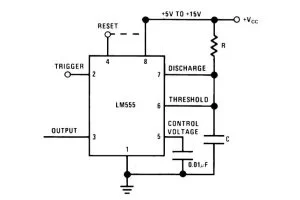
In monostable mode the 555 timer outputs a high pulse, which begins when the trigger pin is set low (less than 1/3Vcc, as explained in the previous step, this is enough to switch the output of the comparator connected to the trigger pin). The duration of this pulse is dependent on the values of the resistor R and capacitor C in the image above.
When the trigger pin is high, it causes the discharge pin (pin 7) to drain all charge off the capacitor (C in the image above). This makes the voltage across the capacitor (and the voltage of pin 6) = 0. When the trigger pin gets flipped low, the discharge pin is no longer able to drain current, this causes charge to build up on the capacitor according to the equation below. Once the voltage across the capacitor (the voltage of pin 6) equals 2/3 of the supply voltage (again, as explained in the previous step, this is enough to switch the output of the comparator connected to pin 6), the output of the 555 is driven back low. The output remains low until the trigger pin is pulsed low again, restarting the process I’ve just described.
(Voltage across Capacitor) = Vcc * (1- e-t / (R*C))
this equation describes the time it takes to charge a capacitor of capacitance C when it is in series with a resistor of resistance R
as explained above, we are interested in the time it takes for the voltage across the capacitor to equal 2/3Vcc, or:
2/3*Vcc = Vcc * (1- e^-t / (R*C))
which can be rearranged to:
2/3 = 1- e-t / (R*C)
e-t / (R*C) = 1/3
-t / (R*C) = ln(1/3)
t = 1.1*R*C seconds
In the next step I’ll connect an indicator LED to the output pin of the 555 and pick some arbitrary values for R and C to make sure that this really works.
Source: 555 timer in different modes of operation with circuit diagram
- How does the 555 timer operate in monostable mode?
An external trigger causes the timer to output a single pulse of adjustable duration based on resistor and capacitor values. - What determines the frequency in astable mode?
The output switches between high and low states at a tunable frequency determined by the circuit configuration. - Can the 555 timer be used directly with a speaker?
Yes, its output can be wired directly to a speaker, making it a great starting point for audio projects. - What are the supply voltage requirements for the 555 timer?
The positive supply voltage should be between 5 and 15V. - How is the reset function achieved on the 555 timer?
The timing of a high pulse can be manually reset by pulsing the reset pin low. - What role do the internal 5kOhm resistors play?
They create a voltage divider that sets reference voltages of 1/3Vcc and 2/3Vcc for the comparators. - Does the discharge pin drain charge from the capacitor in monostable mode?
Yes, when the trigger pin is high, the discharge pin drains all charge off the capacitor. - What equation calculates the pulse duration in monostable mode?
The duration is calculated using the formula t = 1.1 * R * C seconds.