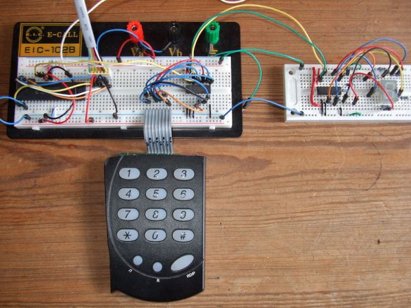
I2C keypad
This instructable explains how to interface with a 4×4 keypad over an I2C bus.
I started this project because I wanted some plug and play input and output modules for easy and fast prototyping of my electronics projects (mostly with PIC microcontrollers). Of course you can use leds and dip switches but they require lots of pins on your microcontroller and you only have binary I/O.
To solve this problem I decided to use I2C.
I2C is a 2 wire bidirectional bus to which addressable devices can be connected.
I had some I2C remote I/O expander chips laying around that I could use for this purpose.
You give them an address and then you can read or write to their 8 I/O pins.
I also recovered a 4×4 keypad from a broken telephone to be used as input device.
And I connected a 7 segment display to the I2C bus as an output device.
In a next iteration of the project I’ll move the components to PCB.
Step 1
Components
Required components:
-1x PCF8574 I2C chip (remote 8-bit I/O expander for I2C-bus)
-1x 4×4 Keypad
-2x 2,2 kOhm pull-up resistors
-1x PIC18F4550 (or other programmable I2C master device)
Optional components (depends on output):
-1x PCF8574 I2C chip
-1x 7 segment display
-7x 330 Ohm resistor
-1x serial to usb dongle
Step 2
Circuit
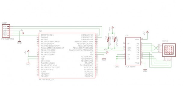
The 8 I/O pins of the I2C chip are connected to the 8 pins of the keypad. It’s easier for writing the code if we make the connections in a logical order. I connected the column pins on one side of the chip and the row pins on the other side of the chip.
Data (SDA) and clock (SCL) from the I2C chip are connected to the data and clock pin of the MCU.
Both SCL and SDA lines are “open drain” drivers. What this means is that the chip can drive its output low, but it cannot drive it high. For the line to be able to go high you must provide pull-up resistors to the 5v supply. There should be a 2,2 kOhm resistor from the SCL line to the 5v line and another from the SDA line to the 5v line. You only need one set of pull-up resistors for the whole I2C bus.
3 bits of the 8bit address of the device are set by connecting the address pins to 5V or to ground.
Output:
The serial output (UART/rs232) goes to my serial to usb dongle that is connected to my pc.
The second PCF8574 chip is connected to the I2C bus by connecting the data and clock line to the data and clock line from the first chip.
For the second chip we need a different address so I connected the first address pin to 5V instead of the ground.
The common anode of the 7 segment display is connected to the 5V from the power source. The other pins are connected with the I/O pins of the I2C chip (using 330 Ohm current limiting resistors).
Step 3: Code
The code implements the standard keyboard scanning routine by reading and writing to the I2C chip. The keypad is scanned by selecting a column and then reading the rows to see wich one of the buttons is pressed.
For more detail: I2C keypad using PIC18F4550 microcontroller


