Getting Ready
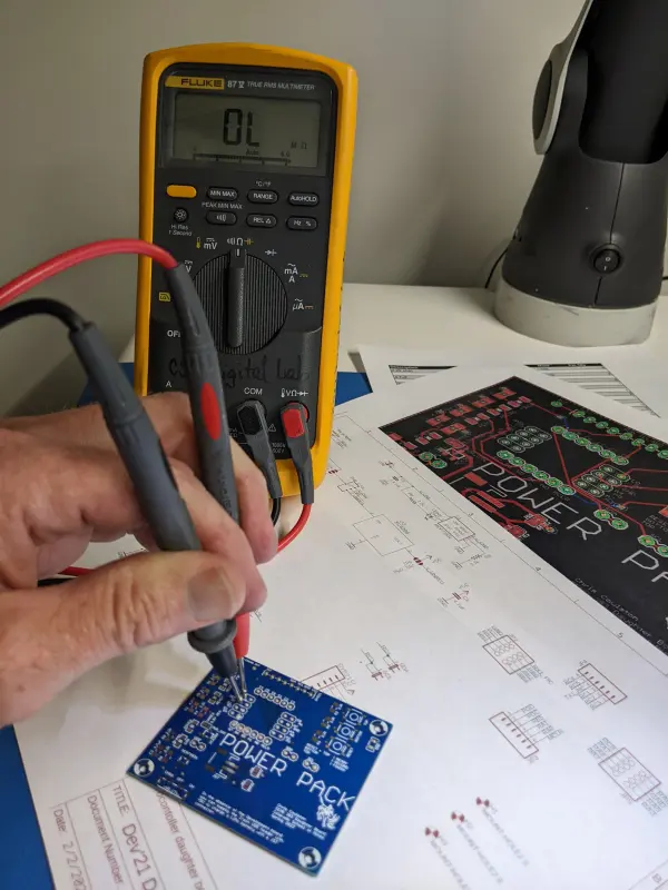
Let’s initiate by conducting a basic test to ensure the accurate manufacturing of your PCB – checking for any potential short circuits between the power and ground rails. Employ the bench digital multimeter to assess the resistance between Vcc and GND. Follow the “Measure Resistance” protocol provided in the inLab, and probe the Vcc and GND pins adjacent to the PIC footprint (as illustrated in the image below). You should register a notably high resistance (indicative of an open circuit). If the reading shows 1Ω or lower, cease the assembly process and acquire a new PCB, as yours might contain a critical flaw. It’s worth noting that encountering a PCB with a short between the power rails is rare, but there’s always a possibility, albeit minimal.
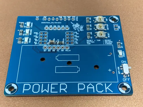
A recommended initial step involves arranging your components in a secure location, following the grouping illustrated in the parts diagram. This method facilitates easy identification of the necessary parts when they are required. It’s important to note that the parts diagram linked above corresponds to an earlier board revision, so there might be slight variations in the number of capacitors and other elements.
To begin, gather a parts tray, solder paste, a solder paste dispenser, a dispenser needle, magnifying goggles, and a pair of tweezers. The solder paste is stored in the small black refrigerator located in Brown 328. Ensure the solder paste is returned to the refrigerator after use. Additionally, allocate at least 2 hours of uninterrupted time for the soldering process of surface mount components.
Organize the parts into two categories: through-hole and surface mount. The surface mount components will be soldered using the reflow skillet technique, while the through-hole components will be soldered later using a soldering iron.
Through-hole components feature extended pins that pass entirely through the printed circuit board. Keep these components in their bag for later soldering.
Surface mount components have small metallic extensions or end caps designed to rest on the surface of the printed circuit board. These smaller parts are often packaged in paper tape. Carefully remove them from the tape using tweezers and remove the clear cover from the top of the tape.
Inspect and arrange the parts from the bag, aligning them on the Parts Diagram to ensure all parts are present. Make a note of any missing components. If a component is missing, inspect the back of the speaker, as sometimes components can stick to its magnet. If there are one or two missing components, proceed with the assembly and plan to hand-solder the missing parts later, with assistance if required.
Subsequently, transfer all surface mount components listed in the Parts Diagram into the black parts tray. Return the through-hole parts to their plastic bag for later use. You might consider removing the surface mount parts from their tape holders for ease of reference. For instance, tape-form capacitors can be placed in the tray for quick value identification. Unlike resistors, capacitors lack clear labeling, potentially causing confusion during placement.
Now, prepare the solder paste “gun” for use. Begin by pressing the oval button atop the gun and pulling the plunger entirely back into the gun’s body. Remove the black cap from the solder paste tube and securely attach a black syringe needle to the dispensing end of the tube by twisting it into place.
Attach the solder paste tube to the gun, ensuring a secure connection, and squeeze the trigger until the plunger reaches the red gasket inside the solder paste tube. Gradually squeeze the trigger until a small amount of solder paste emerges from the dispenser, signifying readiness.
Start by applying a small amount of solder paste to all the two-terminal device pads. The solder paste dab should be approximately the size of a hamburger on a plate—avoid excessive amounts. On the ON/OFF switch, minor solder spillage onto adjacent pads is acceptable. Do not worry about solder bridges at this stage; they can be corrected later.
Place your parts on the board
To avoid accidentally disturbing already placed parts, start by positioning the smallest parts first, followed by larger ones. Begin with the 1206 discretes, then move on to the ICs, and finally, place the mechanical parts. Taking the time now to double-check the correct location and orientation of each part will save time and prevent frustration later in the assembly process.
Progress in placing the components should start from the center of the board and move towards the edges. This sequential approach minimizes the risk of disturbing components already placed on the board.
For resistor orientation, ensure that horizontally-oriented resistors have readable text from the bottom side of the board, while vertically-oriented resistors display readable text from the right side. Consistency in resistor orientation is more critical than the designation of what is considered the bottom or right side of the board.
When there are multiple parts of the same value (e.g., 10k resistors), place all of them at once. This approach helps in accurate part accounting and prevents incorrect placements.
Apply a small amount of solder paste to each pad. The appropriate quantity should resemble a large hamburger on a dinner plate, not an excessive amount akin to a Thanksgiving turkey or an Oreo cookie.
If there’s a high demand for the solder paste, it might be beneficial to apply paste to all pads and place the components later. The paste will not dry out, ensuring flexibility in component placement. If you have exclusive access to the equipment, you can alternatively apply solder paste to pads of a specific component type (e.g., 10k resistors) and then place only those components.
Use tweezers to handle and position small components onto the pasted pads. Employ a two-handed approach, with one hand holding the tweezers and the other hand supporting the first. Avoid pressing or forcing components onto the board as it may cause complications during the reflow process. Components will naturally settle into the solder pool during reflow.
After placing several components, your board may appear imperfect. However, this is not a cause for concern, as the solder paste volume will decrease significantly during reflow. The surface tension of the liquid solder will automatically align the components. To view the images in the table below more clearly, right-click on the image and select “open image in new tab” or use your browser’s equivalent option.
Apply solder paste evenly across each push button pad, taking note of the quantity of paste applied on the pads.
For the SOT23-5 device, create a small “worm” of solder paste spanning the 3 pins. The surface tension of the solder will naturally draw it back to the pins, preventing solder bridges during the soldering process.
Carefully position the SOT-23-5 device; this precision during placement will prevent the need for chip desoldering in later stages.
All LEDs might appear identical. To differentiate between colors, utilize a Digital Multimeter (DMM) in diode checking mode to illuminate them. These LEDs are reused and may show signs of wear. Remember, the green marker on the LED always indicates the cathode (negative end).
The arrow-shaped silk screen symbol near the LED denotes that the cathode is on the right side in the image. Align the LEDs accordingly for easier placement.
The JST connector requires meticulous alignment to ensure the concealed terminals align perfectly with the PCB pads.
Once all components are placed, the board is prepared for the reflow skillet!
Double-check the LED orientation, identifying the cathode by locating the green strip along the lens edge.
Refer to the table below for LED colors corresponding to their silk screen labels:
| Silk Screen Label | Color |
|——————-|———|
| POWER | Green |
| READY | Yellow |
| RECORD | Green |
| FINISH | Red |
Now, proceed to reflow your board.
Reflow your board.
During the subsequent phase of the assembly, you’ll be employing a commercial-grade cooking skillet to heat your development board. The application of heat to the solder paste will initiate a drying phase followed by a transition into molten solder when reaching the appropriate temperature. This transformation from the semi-fluid solder paste to molten solder is commonly referred to as “reflow.” Below is a time-lapse video demonstrating the reflow process of a distinct development board, lasting approximately 6 minutes. In the video, an excess of solder paste was applied, leading to the creation of visible solder bridges by the conclusion.
To ensure an appropriate reflow process for your board, it’s crucial that the reflow skillet begins at a temperature low enough to be touchable with your bare hand. To check the skillet’s temperature, start by placing a solitary drop of water on its surface. If the water drop remains without evaporating for 10 seconds, you can cautiously touch the skillet to assess its temperature. Prior to initiating the PCB reflow, ensure any water on the skillet surface is removed.
Carefully position the pasted PCB onto the reflow skillet. It’s possible to reflow multiple PCBs simultaneously – sharing the skillet is beneficial!
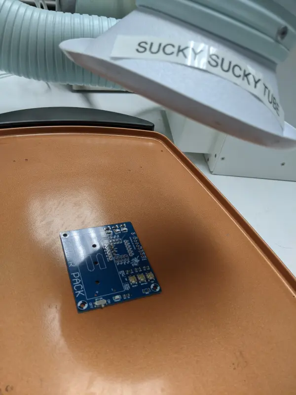
Place the air cleaner (vacuum tube) head over your PCB, ensuring careful handling to avoid any contact or interference between the PCB and the air cleaner tube. Please be aware that the image displays an older version of the board.
Adjust the skillet temperature knob to reach 400 degrees.
Avoid using the Mantis to observe your board during reflow, as it could potentially damage this costly equipment.
After approximately 2 minutes, the PCB will gradually warm up, causing the solder paste to spread evenly across the pads, seemingly melting due to the heat.
Around the 4-minute mark, the solder paste will have dried to a baked consistency. At this stage, slight traces of smoke might emerge from beneath the PCB. While this initially caused concern, I’ve concluded that this occurrence is normal and does not harm the bottom-side solder mask. Please note that the image depicts an older version of the board.
Approximately 6 minutes into the process, the solder paste in warmer regions or spots with minimal thermal mass began to undergo reflow.
By the 8-minute mark, complete solder flow should occur. Before turning off the heat, ensure that all solder paste has transitioned from a dull grey appearance to shiny metallic blobs. At this point, it’s time to switch off the heat on the skillet. Any solder bridges that might have formed can be addressed after the board has cooled down. Please note that the image depicts an earlier version of the board.
Allow the board to rest for approximately 2 minutes after switching off the heat source. Then, using hemostats, carefully move the board towards the edge of the skillet that features a trough. Lift the board cautiously, positioning one side on the raised edge of the skillet while the opposite edge rests on the skillet surface. This arrangement facilitates airflow beneath the board’s edge, expediting the cooling process.
Maintain this position for an additional 2 minutes before using hemostats to lift the board and place it on a cardboard surface, such as a notebook. Caution is advised as the board might still retain enough heat to cause burns.
After letting the board sit for approximately 2 more minutes, it should have cooled sufficiently for a rudimentary temperature check by touch – although not the most precise method. Once the board is cool enough to handle, proceed with any necessary touch-up work.
Fixing Problems on Your Board
Once the solder paste on your board has undergone reflow and has cooled down sufficiently for handling, it’s essential to conduct a thorough visual inspection. Your aim is to spot any faulty solder joints, which can include joints that fail to establish an electrical connection between the device terminal and the PCB (referred to as a “dry joint”), or joints that connect two or more adjacent device terminals (known as a “solder bridge”). Additionally, there might be instances where a component is mistakenly installed backward or where the positions of two identically sized parts are swapped.
Irrespective of the issue, the responsibility falls on you to rectify it. Presented below are some guidelines to address these specific types of problems.
Removing Solder Bridges
Solder bridges occur when excess solder paste is applied to the PCB, causing solder masses to connect adjacent device terminals (pins) during the reflow process. This unintended electrical connection between pins is noticeable as a visible blob of solder between IC pins. It’s noteworthy that solder bridges rarely form beneath an IC or discrete component.
Should you encounter solder bridges, their removal becomes necessary. It’s one of the more challenging techniques in soldering, but with adequate preparation, success becomes more achievable. To address this issue, you’ll require a soldering iron, solder flux, and some solder wick.
Removing Solder Bridge – Step #1
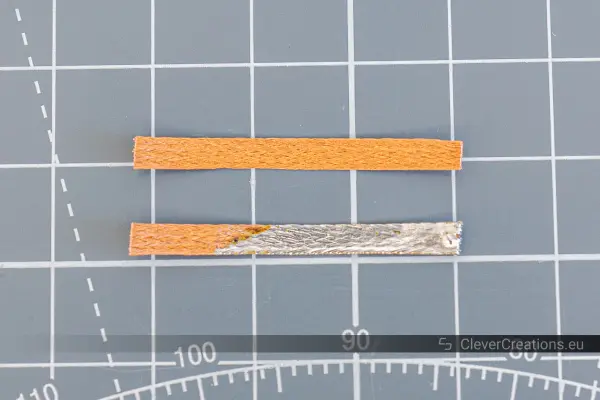
Trim a section of solder wick measuring 1 to 2 inches. Securely grip this piece of solder wick with hemostats. Twist the wick around the tip of the hemostat once or twice to firmly hold it in place. Using the soldering iron, heat the end of the solder wick and apply some solder onto it. The aim is for the solder to penetrate the fabric of the solder wick. This process, known as tinning, resembles wetting a new dry sponge before initial use. Properly tinned wick should resemble the lower piece of solder wick depicted in the subsequent image.
Removing Solder Bridge – Step #2
I prefer working under the Mantis or using head loop magnifiers for better lighting and magnification while desoldering. Next, apply a pool of solder flux to the solder bridge and the adjacent pins. This pool serves a dual purpose: it helps maintain the cleanliness of the solder connection and, more significantly, facilitates the transfer of heat from your soldering iron, through the solder wick, to the solder bridge.
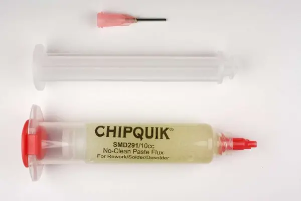
To release solder flux using the flux pen, softly press the tip onto the solder bridge. The pen’s tip is spring-loaded, and a slight in-and-out movement will dispense the solder flux. For the syringe, gently push the plunger to dispense the flux, but exercise caution. As the flux starts flowing, you’ll notice a significant reduction in plunger resistance. If there’s a bit of a mess, don’t fret; after test #8, you’ll utilize the ultrasonic cleaner to eliminate any remaining solder flux residue from your board.
Removing Solder Bridge – Step #3
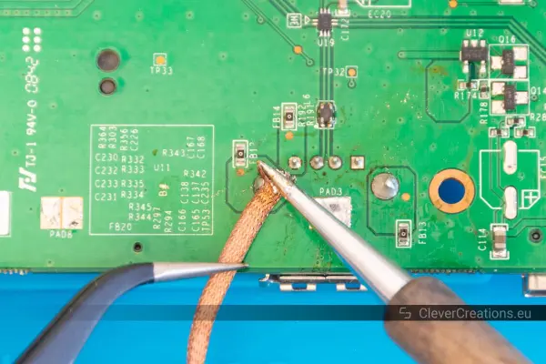
Place the solder wick’s tinned section over the solder bridge. Then, position the side of the soldering iron on the solder wick covering the solder bridge. This setup should resemble the image provided below.
Ensure the iron remains stationary without moving the wick sideways across multiple pins, as doing so might bend the pins and damage the PCB pads. Watch for solder to quickly travel up into the braid, but be cautious not to apply heat for too long, as excessive heating can remove all the solder from the joint. Once you believe the solder bridge is eliminated, lift the iron and braid away from the PCB together.
Many students underestimate the time required to eliminate a solder bridge. A slow count to 6 and subsequent checking is generally effective. If the solder wick sticks to the PCB upon iron removal, refrain from pulling it forcefully, as this might damage the pins and pads. Instead, gently reheat everything and remove the wick when it comes off easily.
While troubleshooting their development boards, students often concentrate on rectifying solder bridges. However, insufficient solder can also pose a significant issue! Ensure the IC pins are securely soldered to avoid potential problems caused by inadequate soldering.
Adding Solder
Surprisingly, identifying an inadequate amount of solder at a solder joint poses one of the most challenging issues. This problem commonly arises with IC and USB pins. It happens due to insufficient application of solder paste on the PCB or when excessive solder is removed while addressing a solder bridge.
To detect a pin lacking sufficient solder paste, use a small, sharp, and firm object, such as the tips of your tweezers, to gently attempt to move the pin. If the pin wiggles upon pressing, it indicates the need for additional solder to be added to that particular pin.
Adding Solder – Step #1
Interestingly, I apply solder using the solder paste gun. I place a small amount of cool solder paste onto both the pin and the pad. If the paste happens to touch neighboring pins, I don’t fret because the solder paste volume significantly decreases upon liquefaction. Then, I employ a hot soldering iron to “reflow” this small solder paste portion. Occasionally, it can be challenging to make the solder adhere to the pin. If you encounter difficulties, don’t hesitate to clean the soldering iron tip thoroughly, consider adding solder flux, and attempt the process again.
Removing Components
If a component has been inserted in the wrong orientation or if two components of identical size have been inadvertently swapped, the removal of one or more components becomes necessary.
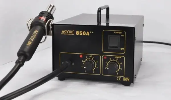
Using a soldering iron is generally not advisable in such situations. Instead, consider utilizing the hot-air rework station depicted in the image below. This rework station comprises a metal box housing an on/off switch, airspeed adjustment, and heater settings. The hand unit is equipped with a plastic handle and a metal tip from which hot air is emitted.
Take note of the hand unit’s positioning in the provided image: ensure that the metal tip, which emits the hot air, is directed upwards and away from any potentially flammable surfaces, such as the desk. This emphasis is crucial as it’s easy to incorrectly position the hand unit with the tip pointing towards the desk. While it’s usually challenging to ignite a desk under normal circumstances, the hot air rework station has the potential to cause such hazards. Therefore, careful handling and positioning are essential to prevent any accidental fire incidents.
Removing Components – Step #1
Activate the hot air station and adjust both the air and heater controls to level 5. Ensure the stability of your board to prevent any movement. Remove any flammable items from the vicinity of your board for safety purposes.
Removing Components – Step #2
Maintain a distance of approximately 1-2 inches between the nozzle and the board’s surface while gently maneuvering the tip around the pins of the components intended for removal. Focus specifically on the pins, avoiding contact with the component body. It’s essential to note that the hot air will also affect nearby components, potentially causing inadvertent reflow of small, two-leaded components nearby. Therefore, exercise caution and direct the stream of hot air away from these neighboring components to minimize their exposure to heat.
Removing Components – Step #3
After approximately 20 seconds, the component will begin to loosen. Continue applying swirling heat while, using tweezers in your other hand, gently lift the part. If you happen to drop the part, there’s usually no need for concern as I’ve observed that the pins tend to cool rapidly as they descend, and the component typically doesn’t adhere to other surfaces. You can place the part on the blue anti-static mat without worry as it doesn’t generate enough heat to cause damage to the mat.
Removing Components – Step #3
Switch off the hot-air rework station. The station will run for a period as it cools down the heating element.
Please refrain from soldering the through-hole components at this stage. Incremental soldering of these components will be necessary as you progress through subsequent tests. Each test will specify the addition of specific through-hole parts required for that particular test.
Test #1 – Test the power subsystem.
Procedure:
To ensure the daughter board powers up correctly in the subsequent step, it’s essential to verify the resistance between Vcc and GND falls within the designated range and that the ON/OFF switch functions properly. Follow these steps to perform the verification:
1. Attach a red probe and a black probe to the benchtop digital multimeter (DMM). Ensure the red probe is inserted into the “V Ω” jack and the black probe into the “COM” jack.
2. Press the “Ω” button on the DMM to activate the resistance measuring mode.
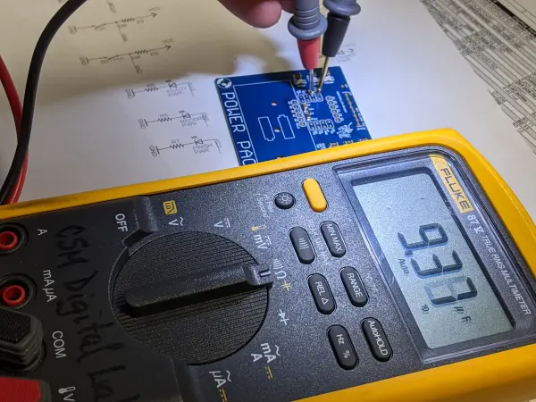
3. Utilize the probes to test the Vcc and GND breakout header holes positioned around the PIC, as depicted in the image below. For a larger view of the image, right-click and select “Open in new tab.”
Commence by setting the ON/OFF switch to the OFF position. When the switch is in the OFF position, there should be no resistive connection between Vcc and GND. The sole connection between Vcc and GND should be through the capacitors soldered to the daughter board. By measuring the capacitance, as indicated below, you should obtain a value relatively close to 10µF. Please note that the image displayed represents an older version of the board.
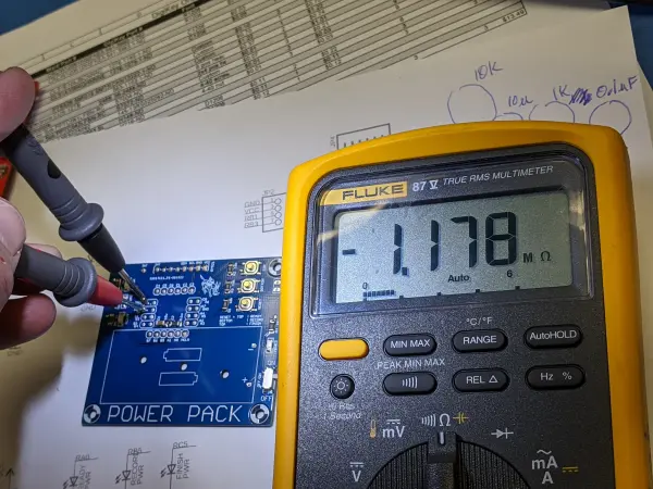
An appropriately assembled daughter board will display a resistance value that fluctuates within the MΩ range, potentially showing negative values, as illustrated in the image below. Please be aware that this image depicts an older version of the board.
If the resistance on the daughter board is low, measuring less than 5Ω, it indicates a short circuit between Vcc and ground. This issue typically arises due to either a solder bridge or an incorrectly placed component. Regardless of the specific cause, identifying and rectifying this problem is essential before continuing further.
Test #2 – Install Test Firmware onto PIC18F25K22
Soldering:
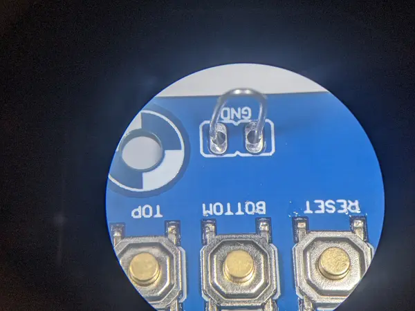
Solder the GND loop by utilizing a discarded resistor. Trim the lead on one side (consider sharing the other side with someone else). Fold the lead in half and carefully insert it into the daughter board, ensuring that the lead forms a loop approximately 7mm above the board’s surface. Proceed to solder it securely into position.
Procedure:
To load the daughter board test program onto the PIC, follow these steps:
1. Open MPLab X.
2. Create a directory on your network drive at /EENG383/lab/lab14.
3. Download Lab14.X.production.hex into the lab14 directory by right-clicking on the link and selecting “Save link as…” or similar, based on your browser.
4. Go to File → New Project.
5. In the New Project window (Step 1: Choose Project),
– Categories: Microchip Embedded
– Projects: Prebuilt (Hex, Loadable Image) Project
– Click Next.
6. In the New Project window (Step 2: Create Prebuilt Project),
– Prebuilt Filename: Navigate to /EENG383/lab/lab14/Lab14.X.production
– Device: PIC18F25K22
– Hardware Tool: SN: BURxxxxxxxxx (where x’s represent your PICkit 3 ID)
– Click Next.
7. In the New Project window (Step 3: Select Project Name and Folder),
– Project Name: Lab14.X.production.prebuilt (default)
– Project Location: \EENG383\lab\lab14 (default)
– Click Finish.
8. Connect the USB cable between your PC and the development board.
9. Attach your programmer to both your PC and the development board.
10. Click the green Play button located in the toolbar at the top center of the screen.
11. Acknowledge the MPLAB caution pop-up by clicking OK (“CAUTION: Check that the device….”).
12. In the console area at the bottom of the MPLab X window, observe the following activity within a tab labeled “PICkit 3” or “PICkit 4” or “SNAP”.
*****************************************************
Connecting to MPLAB Snap...
Currently loaded versions:
Application version…………00.04.50
Boot version……………….01.00.00
Script version……………..00.04.48
Script build number…………7acb7c9d66
Tool pack version ………….1.7.510
Target device PIC18F25K22 found.
Device Id Revision = 0x5
Calculating memory ranges for operation…
Erasing…
The following memory area(s) will be programmed:
program memory: start address = 0x0, end address = 0x303f
program memory: start address = 0x7740, end address = 0x7fff
configuration memory
Programming/Verify complete
Once the programming is completed, disconnect the SNAP programmer. Next, connect the development board to a PC and initiate PuTTy. Establish a connection with the appropriate serial port, and type “?” to prompt a menu displaying the commands necessary for testing the daughter board. You should expect to observe something resembling the following:
-------------------------------------------------
?: Help menu
Z: Reset processor
z: Clear the terminal
d: Program documentation
-------------------------------------------------
i: Initialize SD card
-/+: decrease/increase read address
r: read a block of 512 bytes from SD card
-------------------------------------------------
o: reset accelerometer
A: read all the registers from the MPU6050
a: read acceleration data registers from the MPU6050
g: read gyroscope data registers from the MPU6050
W: Write an arbitrary MPU6050 register and value
R: Read an arbitrary MPU6050 register
-------------------------------------------------
b: test daughter board Buttons
l: test daughter board LEDs
-------------------------------------------------
Test #3 – Test Buttons
Soldering:
You’ll be soldering the female headers responsible for connecting the daughter board to the development board. These include 2 6-pin headers, 2 2×4 headers, and 1 2-pin header. Achieving a perpendicular alignment to the surface of the daughter board is the primary challenge in this task.
I find the following method to be highly effective:
Position all the headers onto the development board in their respective places.
Position the daughter board directly over the headers, ensuring an exact alignment of the daughter board outline with the designated area. It might take some time to properly guide the daughter board onto the pins, as achieving precise alignment can be challenging. Once a couple of pins have engaged, gently wiggle the daughter board while applying slight pressure to ensure a secure fit.
Verify that the daughter board is level with the development board by gently pressing down, ensuring it is not slightly tilted under its own weight.
Initiate soldering by soldering one pin on the header, preferably choosing one of the end or corner pins. Reference the accompanying images to assist in guiding the soldering process for the header pins. For clearer visuals, right-click on the image in the table below and select “open image in new tab” or use your browser’s equivalent option.
Explaination of the pictures
Position the soldering iron in a manner that places its flat chisel tip against the PCB, applying gentle pressure against the header pin’s flat side. Maintain this fixed position throughout the soldering process until its completion.
Prepare the solder by applying a small amount to the iron’s tip initially to facilitate heat flow. Once the soldering area reaches an optimal temperature and the solder begins to melt, delicately tap the solder against the header pin in small increments. Aim for the solder to form a shape resembling a Hershey’s Kiss. Over-soldering may result in an undesirable onion dome appearance.
After applying the solder, withdraw the solder and allow the iron to remain in place for 2-3 seconds, encouraging the solder to seep down into the PCB barrel that secures the header pin.
Remember to solder the 2-pin header located near the JST connector.
Prior to soldering additional pins, verify that the daughter board aligns evenly with the development board. If necessary, reheat the soldered pin to make any necessary adjustments. Once a second pin is soldered, making alterations becomes significantly challenging.
Once you’ve confirmed proper alignment, proceed to solder the remaining header pins.