
Summary of How to work with inbuilt ADC Module of PIC18F4550
This article explains the built-in ADC module of the PIC18F4550 microcontroller, covering its 10-bit resolution, 13 analog channels, external Vref pins, selectable clock options, and auto-triggering capability. It details ADC-related registers ADCON0 and ADCON1, describes bits for enabling the ADC, starting conversions, selecting channels (CHS0–CHS3) mapped to specific pins, and configuring pins as analog or digital via PCFG bits and VCFG reference selections.
Parts used in the PIC18F4550 ADC Module Project:
- PIC18F4550 microcontroller (with inbuilt ADC)
- Analog transducers/sensors (external)
- Vref+ (RA3) external reference connection
- Vref- (RA2) external reference connection
- Power supply for PIC (Vdd, Vss)
- Connecting wires / PCB traces for analog channel pins
- Optional: clock source or oscillator for the PIC
- Optional: pull-up/pull-down resistors for I/O as needed
A microcontroller, a digital device, can read, execute and transmit only digital signals. On the contrary, the outputs of the most of the transducers are analog in nature. Thus it is hard to interface these transducers directly with controllers. Analog-to-digital convertor (ADC) ICs are one way to make the analog input compatible with the microcontroller.
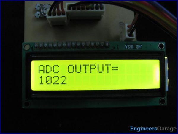
Using an external ADC adds complexity to the circuit. To avoid this complexity, PIC Microcontrollers have in-built ADC module which reduces the cost and connections of the circuit. This article explains the in-built ADC of PIC18F4550 controller.
As mentioned in the summary, a PIC microcontroller has inbuilt ADC for A/D conversion. The ADC module of PIC18F4550 controller has following specifications:
|
Bit 7
|
Bit 6
|
Bit 5
|
Bit 4
|
Bit 3
|
Bit 2
|
Bit 1
|
Bit 0
|
|
—
|
—
|
CHS3
|
CHS2
|
CHS1
|
CHS0
|
GO/DONE
|
ADON
|
|
CHS3:CHS0
|
Analog Channel
|
Pin
|
|
0000
|
Channel 0
|
RA0/AN0
|
|
0001
|
Channel 1
|
RA1/AN1
|
|
0010
|
Channel 2
|
RA2/AN2
|
|
0011
|
Channel 3
|
RA3/AN3
|
|
0100
|
Channel 4
|
RA5/AN4
|
|
0101
|
Channel 5
|
RE0/AN5
|
|
0110
|
Channel 6
|
RE1/AN6
|
|
0111
|
Channel 7
|
RE2/AN7
|
|
1000
|
Channel 8
|
RB2/AN8
|
|
1001
|
Channel 9
|
RB3/AN9
|
|
1010
|
Channel 10
|
RB1/AN10
|
|
1011
|
Channel 11
|
RB4/AN11
|
|
1100
|
Channel 12
|
RB0/AN12
|
|
Bit 7
|
Bit 6
|
Bit 5
|
Bit 4
|
Bit 3
|
Bit 2
|
Bit 1
|
Bit 0
|
|
—
|
—
|
VCFG1
|
VCFG0
|
PCFG3
|
PCFG2
|
PCFG1
|
PCFG0
|
- What is the resolution of the PIC18F4550 ADC?
The ADC provides a 10-bit resolution output. - How many analog channels does the PIC18F4550 ADC have?
There are 13 analog channels available (channels 0 to 12). - Which pins are used for external reference voltages?
Vref+ is on RA3 and Vref- is on RA2 for external reference voltage connections. - How is the ADC enabled or disabled?
ADC is enabled or disabled using the ADON bit in the ADCON0 register (1 enables, 0 disables). - How do you start an A/D conversion?
Set the GO/DONE bit in ADCON0 to 1 to start conversion; it clears to 0 when conversion is complete. - How are analog channels selected?
Channels are selected using CHS3:CHS0 bits in ADCON0 according to the channel-to-pin mapping table. - Can ADC pins be used as digital I/O?
Yes; PCFG3:PCFG0 bits in ADCON1 configure multiplexed pins as digital I/O or analog inputs. - Are there selectable ADC clock options?
The ADC offers 8 selectable clock options for conversion timing. - Does the PIC18F4550 support continuous ADC conversions?
Yes, the ADC can operate in auto-triggering mode for continuous A/D conversion.
