Summary of How to Implement SPI Using PIC18F4550
The article explains implementing SPI on PIC18F4550, describing SPI basics, MSSP registers (SSPBUF, SSPSTAT, SSPCON1), read/write behavior, and coding tips. It outlines master/slave roles, clock behavior, and provides code for a master that exchanges data with a slave and displays sent/received bytes on a 16x2 LCD.
Parts used in the Implement SPI Using PIC18F4550 Project:
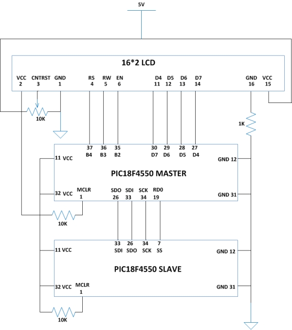
- PIC18F4550 microcontroller (master and slave)
- 16x2 LCD display
- Connections for SPI bus: SDO (MOSI), SDI (MISO), SCK (Serial Clock)
- SS (Slave Select) pin
- Power supply (Vcc, ground)
- Wiring/header pins for PORTB and PORTD (LCD control and data)
- Clock source (internal oscillator configured via OSCCON)
The Serial Peripheral Interface (SPI) is a high speed, synchronous, serial communication standard. This communication protocol is basically a Master – Slave implementation where the master device controls the clock based on which the slave devices operate. The master communicates with a slave or a number of slaves in a system through the SPI bus.
The SPI bus requires a minimum of three wires including SDO (Serial Data Out), SDI (Serial Data Input) and SCK (Serial Clock). Since it is a master controller system the SDO is also called MOSI (Master Output Slave Input) and the SDI is also called MISO (Master Input Slave Output).
The SPI is a full-duplex high speed communication protocol. The master and slave can transmit and receive data at the same time. The master is the device which generates clock for all these data transmissions.
Read PIC microcontroller tutorial based on PIC18F4550 microcontrollers in which one of the microcontroller acts as a slave transmitter and the other acts as master receiver.
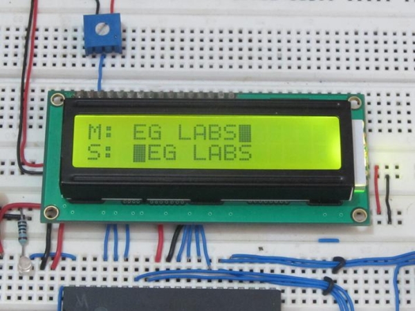
With the help of an LCD, this particular project demonstrates the complete data transfer between a master and slave when both the master and slave are transmitting and receiving the data at the same time.
In PIC18F4550 microcontroller the hardware implementation for the SPI interface can be viewed as a simple SISO (Serial-In-Serial-Out) Shift register controlled by a Clock.
The above diagram is a single buffer implementation of the SPI hardware. The data is shifted into the buffer from the slave device through the SDI (MISO) and the data is shifted out of the buffer to the slave through the SDO (MOSI). The only difference in the hardware configuration of a master and slave device is the direction of the clock. For a master device the clock is always output and for a slave device the clock is always input.
The Clock unit can generate the clock required for the data transmission. In case of a master device the clock is generated by the device and all other devices in the SPI bus send or receive data to the master based on this clock. When the microcontroller is configured as a slave it can only accept the clock from a master device.
On each clock generated or received one bit in the SISO register is shifted from the SDI to SDO. After the eighth clock since the communication starts, one byte of data has been shifted out through the SDO and one byte of data has been shifted in through the SDI. Now the SISO has an entire byte received from the slave while transmitting a byte to the slave.
In PIC18F4550 the Serial Communication registers are not dedicated for the SPI only, but it can be configured for IIC communication also. The entire module is called Master Synchronous Serial Port (MSSP) module. There are a few registers available in the PIC18F4550 which helps to configure the MSSP as an SPI master or slave module. The major registers associated with the SPI communication in the PIC18F4550 are SSPBUF, SSPSTAT and SSPCON1 register.
SSPBUF
The Synchronous Serial Port Buffer (SSPBUF) register is the register which holds the SPI data which needed to be shifted out to the slave or which has been shifted in from the slave. In case of a slave device this register holds the SPI data which needed to be shifted out to the master or which has been shifted in from the master.
SSPSTAT
The Synchronous Serial Port Status (SSPSTAT) register is the register which holds the status of the SPI module. The first two bits and the last bit of this register are only dedicated for the SPI communication.
The SMP bit decides when the master should sample the data, the CKE decides when to transmit data based on the clock transition and the value of BF indicates whether the SSPBUF is full or not (reception complete or not).
SSPCON1
The Synchronous Serial Port Control 1(SSPCON1) register is the register which is dedicated register for the control of SPI only. All the bits of these register are significant and should be carefully set them.
WCOL bit indicates whether a Write collision has been occurred or not, the SSPOV indicates whether an overflow occurred in SSPBUF or not, SSPEN is the bit which is used to enable or disable the SPI module. The CKP bit is used to decide which are the idle state and the active state of the clock. The bits SSPM3 to SSPM0 is used to set the device as a master or slave with required clock frequency for master and SS enabled or disabled for the slave.
The registers are explained with more details in PIC microcontroller
READ AND WRITE OPERATIONS
Whenever the master or slave needs to transmit data, it can simply write the data to the SSPBUF. When the master writes the data to the SSPBUF the clock will get generated automatically and with each clock the data from the SSPBUF is shifted out through the SDO pin bit by bit. When the slave writes into the SSPBUF the data remains there until the master generates a clock which will shift the data out from the slave’s SSPBUF through its SDO pin.
Apart from simply writing into the SSPBUF for data transmission, the master or slave can also read the received data from the SSPBUF. The master and slave should write or read from the SSPBUF in a particular manner only. Read PIC microcontroller tutorial to know more.
TIPS FOR CODING:
The SPI protocol is implemented in different devices in different manner and hence when it comes to the coding one should carefully study all the hardware details regarding the SPI implementation in the device for which the coding should be done. Care should be taken especially on the clock frequency, SPI pin’s multiplexed arrangement, clock polarity settings, use of SS pin and code performance etc. To have clear understanding of code writing visit PIC Microcontroller tutorial.
CODE DETAILS
The code includes a few functions for initializing the SPI module, sending and receiving the SPI data etc. The details of the functions are given below;
Voidspi master_init ( void )
This function is used to initialize the SPI module as a master with the required clock frequency. It also set the clock polarity and when to sample input data and to transmit output data regarding the clock transition states. It also sets the SPI pins as input or output as required by the master. It can also disable all other modules multiplexed into the SPI pins.
Voidspi slave_init ( void )
This function is used to initialize the SPI module as a slave with SS pin enabled. It also set the clock polarity and when to sample input data and to transmit output data regarding the clock transition states. It also sets the SPI pins as input or output as required by the slave. It can also disable all other modules multiplexed into the SPI pins.
unsigned char spi data ( unsigned char tx_data )
This function can send a data byte which it takes as the argument and return the received data byte. The master first write the data and then wait for the data to complete transmission and then read the received data while the slave first wait till all the data bits has been received, and then reads the data followed by a data write.
The functions are explained with more details in PIC microcontroller tutorial.
MASTER AND SLAVE AS TRANSMITTER AND RECEIVER
The arrangement below shows how the master transmits some meaningful data to the slave which the slave can receive. The data which the master transmits is displayed in the first line of the 16×2 LCD. The slave then transmits the same data which it has received back to the master which is then displayed in the second line of LCD. In this way the master is doing transmission and reception and the slave is also performing transmission and reception. Since the PIC18F4550 is used as master and slave the capabilities of the SPI module of the PIC18F4550 is exploited to the maximum in this project. The following figure can make the arrangement details more clear;
- What registers are majorly associated with SPI in PIC18F4550?
The major registers are SSPBUF, SSPSTAT, and SSPCON1 as described in the article. - How does data transfer occur on each clock in SPI?
On each clock one bit in the SISO register is shifted from SDI to SDO; after eight clocks one byte is shifted out and one byte is shifted in. - Can the PIC18F4550 MSSP module be used for protocols other than SPI?
Yes, the MSSP module can be configured for IIC communication as well as SPI. - How does the master and slave differ in clock handling?
The master generates the clock (clock is output); the slave accepts the clock (clock is input). - What does writing to SSPBUF do for the master?
When the master writes to SSPBUF the clock is generated automatically and data is shifted out through SDO with each clock. - How should the slave use SSPBUF to transmit data?
The slave writes into SSPBUF and the data remains until the master generates the clock to shift it out via the slave SDO pin. - What do the SMP, CKE, and BF bits in SSPSTAT indicate?
SMP decides when the master samples data, CKE decides when to transmit based on clock transition, and BF indicates whether SSPBUF is full (reception complete). - What control bits are important in SSPCON1 for SPI?
WCOL indicates write collision, SSPOV indicates overflow, SSPEN enables SPI, CKP sets clock idle/active state, and SSPM3:SSPM0 set master/slave mode and clock frequency or SS enable. - Does the project demonstrate full-duplex communication?
Yes, the project demonstrates both master and slave transmitting and receiving data simultaneously and displaying results on the LCD.