Summary of Exploring Leon’s Mini Random Number Generator (mRNG)
The article describes a handheld portable mRNG decision-maker that produces truly random choices from 0–15 (hexadecimal), using a two-button interface and a thumb wheel to set the range. It explains operation, design optimizations for low power, the ATtiny24 microcontroller, a transistor-plus-bandgap-noise random-bit generator amplified by op-amps, debiasing in software, and construction/soldering and casing tips.
Parts used in the mRNG Decision-Maker:
- ATtiny24 microcontroller
- Coin battery and battery holder
- Thumb wheel potentiometer
- Two push buttons (power and freeze)
- Single-digit seven-segment LED display
- 1.2kΩ LED current limiting resistors
- MMBT3904 transistor
- ZXRE1004FFTA 1.22V bandgap voltage reference
- Resistors: 100kΩ (R1), 470Ω (R2), 1MΩ (R3), 100kΩ (R4) and other resistors
- Capacitors (including C3 and C4)
- OPA2340 dual op-amp
- PCB (custom circuit board)
- Case/key fob enclosure
- Surface-mount components and through-hole switch
Sales Pitch
Feeling overwhelmed by choices? Who isn’t? Decision-making can be a maze. White, rye, or wheat? Pinstripes or polka dots? Feast or fast? But fret not—assistance is at hand!
Enter the world’s inaugural, handheld, portable decision-maker, fueled by genuinely random numbers. While my competitors offer decision-makers for 1, 5, 10, or 25 cents, can they navigate choices beyond two? No! Are their decisions authentically random? Absolutely not! My invention accommodates selections from up to 16 options, yielding truly unpredictable outcomes, in line with the principles of quantum (or, at the very least, statistical) mechanics.
Some might object, “But Leon, I’m capable of making my own decisions.” True, yet often, these decisions are arbitrary, lacking logic, and lead to regret. Why anguish over both the choice and its aftermath when you can focus solely on the latter? Embrace novelty! Release your worries! Bid farewell to determinism! Dispel the paradox of choice! Embrace randomness—it might just be the change you need!
Operation
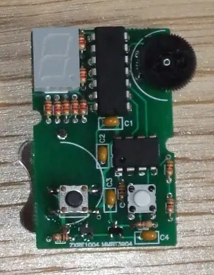
In comparison to most modern complexities, my mRNG operates quite straightforwardly. The device comprises solely two buttons and a single thumb wheel. To operate the mRNG, position it display side up, with the metal ring facing away from you as depicted in the image at the top of the page and demonstrated in the accompanying video.
The left button serves to power on the device. Press and hold this button to activate the device. It rapidly generates a new number approximately 30 times per second, making it too quick for direct reading. Holding down the second button freezes the screen update, enabling you to view the most recent random number generated.
The thumb wheel adjusts the upper limit of the random number range, spanning from 0 to that specific upper boundary. This upper limit can be set to a maximum of 15. Given that the display features only a single digit, the numbers are represented in hexadecimal format (where 10 to 15 are displayed as a-f). Altering the range prompts the new upper limit to be displayed for around 0.75 seconds before the generation of more random numbers resumes. Upon powering on, the device will also briefly display the current upper limit for the same duration.
It’s important to note that ‘6’ and ‘b’ (representing 11 in hexadecimal) might appear similar on the display. However, the distinction lies in the display’s top segment being lit for ‘6’ but not for ‘b’. (Refer to the informative Wikipedia article on Seven-segment display character representations, specifically the left column of characters, for reference.)
Design notes
Fitting all components into a key fob required compactness. This aspect wasn’t inherently challenging, but it necessitated the use of a coin battery. To meet the requirement of drawing 4mA or less (the current version operates at 6-7mA, which is in close proximity), the strategy primarily involved selectively powering different sections of the circuit on and off as necessary. For instance, when generating a random number, the display remains off. The display elements themselves undergo rapid pulsing on and off, creating the impression of continuous activation (ensuring that no more than 4 segments are simultaneously active). Considering this, allow me to delve deeper into the design details. (Access to the source code and comprehensive schematic is available below.)
Microcontroller part
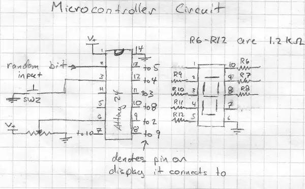
Instead of employing a PIC microcontroller (as I did in my previous project) or sequential logic, utilized in earlier versions, I opted for an AVR. Both had the necessary hardware features, yet the PIC lacked a freely available C compiler compatible with Linux and OS X. While coding in assembly was intriguing, I preferred allocating my time elsewhere. My choice fell on the ATtiny24 due to its appropriate pin count and inclusion of an analog-to-digital converter.
The microcontroller drives the LEDs via 1.2kΩ resistors, a value selected to strike a balance between brightness and low current consumption—although alternative values could also suffice. The switch doesn’t necessitate an external pull-up resistor as the microcontroller integrates internal ones. No efforts were made to debounce the switch as it proved unnecessary. The potentiometer is linked to the microcontroller’s analog-to-digital converter, setting the upper limit of the random number range.
The input for the random bit is connected via a digital input pin. Similarly, no debounce attempt was made, as the average frequency of the random digital output was significantly slower than the microprocessor’s clock speed (1 MHz), rendering timing issues negligible. However, this assessment was conducted solely for the random bit generation circuit without considering the noise from the microcontroller. The software debiases the random digital input using the Von Neuman method and a linear feedback shift register, acting as a randomness extractor.
Operating at 1MHz, the microcontroller utilizes its 8MHz internal oscillator. Potential future versions might leverage the internal 128kHz oscillator to conserve power, though I anticipate the resultant savings to be minimal.
The source code is provided below for reference.
Random bit generating part
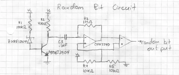
This design drew inspiration from Terry Ritter’s random noise sources, where diodes are commonly employed for generating noise. However, acquiring noisy low voltage diodes is challenging. Hence, to mimic a zener diode, we utilize a 1.22V bandgap voltage reference (the ZXRE1004FFTA).
According to the datasheet, this voltage reference operates optimally with a current of no more than 8μA (typically 4μA), generating the most noise at this current level (refer to page 3). The aim is to run it at a current close to this specification to conserve power and extract maximum noise. Considering the MMBT3904 transistor’s base to emitter voltage drop (~0.75V), the voltage reference’s drop (1.22V), and the supplied battery voltage (~3V), the expected drop across the resistor totals around 1V. Therefore, a 100kΩ resistor (R1) permits approximately 10μA of current flow (likely slightly less due to battery voltage fluctuations).
Given this base current through the transistor and its gain of a few hundred, an anticipated ~2mA should flow through the transistor’s collector. Aiming for an output of approximately 1.5V from the collector (in the middle of the voltage range), a 750Ω resistor suffices. Yet, a nearby resistor value will suffice, so a 470Ω resistor (R2) is chosen, resulting in a drop of approximately 1 volt.
This resultant signal passes through a capacitor for voltage level adjustment and is then amplified by an op-amp. Aiming for a digital signal, an “infinite” gain is sought from the amplifier. However, to maintain equal average voltage levels at the inputs, a very large resistor (1MΩ – R3) is used. Despite the high slew rate of the OPA2340’s output, the signal remains non-digital; hence, it undergoes further amplification by the second op-amp on the chip, achieving a digital output (maximum or minimum voltage). This output is then directed to the microcontroller. Although the output appears to possess an evenly distributed combination of ones and zeros, it undergoes debiasing within the microcontroller for added safety.
Construction
Unless there is specific interest, I won’t delve into intricate details here since the instructions are quite clear (for instance, you’ll notice R4 marked as a 100k ohm resistor, so you’d place it in the spot designated R4 and solder it). However, I can offer some general guidance. If you require fundamental soldering information, there are numerous excellent tutorials available online.
Regarding the surface mount parts, I’ve found an effective method is to apply a small amount of solder to one of the pads, hold the component in place with tweezers, heat the pin so that the solder on the pad adheres to it, and then adjust the component’s orientation as needed while applying heat. Subsequently, you can easily solder the remaining pads. In the realm of surface mount components, these parts are relatively straightforward to handle.
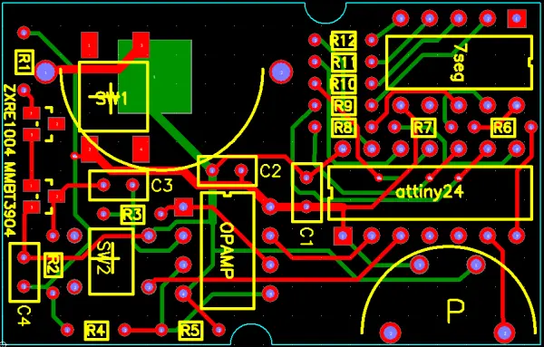
I believe the most effective soldering sequence is to begin with the smallest components and progress to the larger ones. Commence with the ZRE1004 and MMBT3904, followed by the capacitors, then the resistors, and lastly, the larger components. There’s a notable clearance concern with C3, so ensure to trim its leads short before attaching the battery holder to prevent unwanted contact. It’s crucial to solder C3 and C4 before the battery holder; the reverse sequence isn’t feasible.
For components like the display, microcontroller, and op-amp, soldering in the wrong orientation poses a risk due to the absence of sockets. It’s crucial to align pin one with the hole featuring the square pad, near the end where the silkscreen exhibits a notch. Double-check before soldering to avoid errors. Additionally, the through-hole switch must be inserted as far as possible to prevent it from being depressed by the case’s button pad without actual button activation. Sometimes, straightening the switch’s leads before PCB insertion aids in achieving a secure fit.
Once soldering is complete, you’ll need to create two holes in the case—one for the thumb wheel and another for the display. These instructions might seem unclear until you have the case in hand and observe how components fit within it. I recommend using a sharp pocket knife and a punch-and-die type nibbler to craft the holes. Firstly, cut the hole for the thumb wheel at the top part of the case, guided by the alignment of the PCB’s notches with the PCB support posts/screw holes. Then, create a hole for the display using the knife and use the nibbler to form an appropriately sized hole. Ensure a snug fit by cutting gradually and checking the fit repeatedly.
Inside the case’s top section, there are two posts for the buttons’ support to connect to. Remove the top post positioned near the display’s corner, while trimming the button’s support to fit the other post’s connector. Additionally, the PCB support posts on the case’s top half may require minor trimming for a perfect fit, and there might be residual manufacturing nubs inside the case that need removal. An update: I typically use a CNC mill for case openings now, and if you have access to one, it’s highly recommended for this purpose.
- How many options can the mRNG handle?
The device accommodates selections from up to 16 options (0 to 15). - How do you set the upper limit for random numbers?
The thumb wheel potentiometer sets the upper limit, up to a maximum of 15, and the new limit is briefly displayed for about 0.75 seconds. - How do you freeze and read a random number?
Hold down the second button while the device is powered on to freeze the screen update and view the most recent random number. - Why are numbers shown in hexadecimal?
Because the display is a single digit, numbers use hexadecimal representation so values 10 to 15 appear as a to f. - What microcontroller is used in the project?
The project uses an ATtiny24 microcontroller operating at 1 MHz using its 8 MHz internal oscillator. - How is randomness generated and processed?
A noise source using a bandgap voltage reference and transistor produces analog noise, amplified by OPA2340 op-amps to a digital signal, which is debiased in software using the Von Neumann method and a linear feedback shift register. - How was low power consumption achieved?
Power savings are achieved by selectively powering circuit sections, keeping the display off during number generation, and pulsing display segments so no more than four segments are simultaneously active. - What are important assembly cautions?
Solder small components first, trim C3 leads before attaching the battery holder, ensure correct orientation for the display, microcontroller, and op-amp, and fit the through-hole switch fully to avoid misactivation. - Which component provides the noisy reference instead of a zener diode?
The ZXRE1004FFTA 1.22V bandgap voltage reference is used to emulate a noisy zener-like source. - Are switch debouncing and input jitter a concern?
No debounce was implemented for the switch or random digital input because the microcontroller clock is much faster than the random bit frequency, making timing issues negligible for the random input.