


Summary of 2meter (144MHz) amateur radio transceiver
Summary: I designed, built, tested, and operated a 2 meter (144 MHz) ham radio transceiver including VCO+PLL frequency synthesis, LNA receiver front end, 3‑stage PA with harmonic filtering, and a PIC microcontroller interface. All schematics, PCBs, and calculations are in my public git repo (mrf262 and mc3361). The design uses an external Clapp VCO with varicap tuning, LMX2305 PLL, Wilkinson splitter in a second VCO version, and a P16F84A to control frequency and PTT.Parts used in the 2 meter (144MHz) amateur radio transceiver:
- LMX2305 digital PLL I.C.
- Crystal resonator (reference for PLL)
- BFQ19 transistor (Clapp VCO active device)
- BBY40 varicap tuning diode
- MOSFET (VCO output driver in first VCO version)
- Wilkinson power splitter (in second VCO version)
- Operational amplifiers (biasing and modulation circuits)
- Voltage regulator
- Decoupling capacitors
- Low Noise Amplifier (LNA) components
- Three-stage bipolar transistors for Power Amplifier (PA)
- Inter-stage matching coils and tuning capacitors
- Output harmonic filtering network
- 50 ohm input/output RF connectors and transmission line
- P16F84A microcontroller (PIC) running at 4 MHz
- Serial interface circuitry for desktop communication
- Push-to-talk (PTT) switching circuitry
- PCB boards and associated passive components
I designed , built, tested and operated a 2m hamradio transceiver that includes all the necessary circuitry, in particular the voltage-controlled oscillator (VCO) + phase-locked loop (PLL) for frequency synthesis, low noise amplifier (LNA) for the receiver front-end, power amplifer (PA) for the radio frequency (RF) output stage and PIC based micro-controller (PIC) with serial interface to computer desktop. All the schematics , pcb and calculations for this project can be found within the subdirectories of my public git repo dedicated to RF circuits, in particular mrf262 and mc3361.
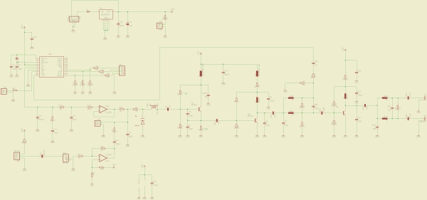 The VCO+PLL has two versions, the first one uses a negative voltage pump generator to supply power to the operational amplifiers responsible for biasing the tuning varicap diode and mixing in the digital/audio modulation and also uses a mosfet as the output driver. The second version includes a Wilkinson power splitter to provide 2 identical power outputs, one for the transmitter board and the other for the receiver board and removes the need for the negative voltage supply. They both use the LMX2305 digital PLL I.C., which needs a stable reference frequency, provided by a crystal resonator and the internal division stages can be controlled through a 3 wire interface directly from a micro-controller or desktop computer. THE PLL I.C. doesn’t include an internal VCO, so a Clapp oscillator had to be designed around a BFQ19 transistor , a small adjustable coil and a BBY40 varicap tuning diode. This circuit block also includes a voltage regulator and a fair amount of decoupling capacitors to obtain a clean output signal.
The PA is a 3-stage bipolar transistor circuit and output harmonic filtering bank, where the inter-stage matching circuits include coils and tuning capacitors, which need to be adjusted for maximum efficiency and power gain. The 50Ω input of this block is connected to the VCO+PLL frequency synthesis block described above and the 50Ω output to the antenna.
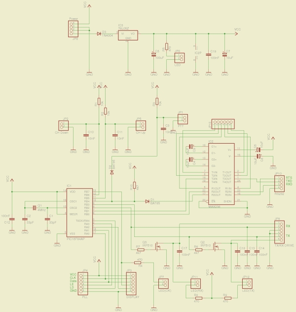 The micro-controller circuit block contains a P16F84A running at 4MHz, with firmware programmed in the assembly language. The firmware is responsible for programming the PLL+VCO circuit block with the transmission frequency when the PTT signal is activated and the RX frequency when receiving since the RX frequency is shifted by the receiver first stage intermediate frequency (I.F.), in this case 10.7MHz.
For more detail: 2meter (144MHz) amateur radio transceiver
- What PLL I.C. is used for frequency synthesis?
The design uses the LMX2305 digital PLL I.C. - Does the PLL include an internal VCO?
No, the LMX2305 does not include an internal VCO, so a Clapp oscillator was designed around a BFQ19 transistor. - How is the VCO tuned?
The VCO is a Clapp oscillator using a BBY40 varicap diode and an adjustable coil for tuning. - Can the PLL division stages be controlled externally?
Yes, the internal division stages can be controlled through a 3 wire interface from a microcontroller or desktop computer. - What provides the PLL reference frequency?
A crystal resonator provides the stable reference frequency for the PLL. - What are the two VCO+PLL versions described?
The first version uses a negative voltage pump and a MOSFET output driver; the second uses a Wilkinson power splitter to provide two identical outputs and removes the need for negative supply. - What does the power amplifier consist of?
The PA is a three-stage bipolar transistor circuit with inter-stage matching coils and tuning capacitors and an output harmonic filtering bank. - How does the microcontroller control the transceiver?
A P16F84A running at 4 MHz programs the PLL+VCO with transmit and receive frequencies and handles PTT switching; firmware is in assembly language. - Where are the project schematics and PCBs located?
All schematics, PCB layouts, and calculations are in the public git repository subdirectories mrf262 and mc3361. - How is the RX frequency adjusted for the receiver I.F.?
The microcontroller programs the RX frequency shifted by the receiver first stage intermediate frequency of 10.7 MHz.
Related projects
Audio Spectrum Analyzer
We developed an audio spectrum analyzer as our final project for ECE 4760. This analyzer presented a histogram-style representation of audio signals....
Audio, Sound & Radio · PIC12F675Audio CRO using PIC12F675 Microcontroller
This project is a miniature Audio CRO. For those not familiar with the abbreviation "CRO," it means "Cathode Ray Oscilloscope" and this...
Audio, Sound & RadioBuild a musical EKG with the Freescale FRDM-KL05
Short Introduction: I have been following the Battle of the DreamBoards Championship with interest and I enjoyed the variation of functionality features...
Audio, Sound & RadioPIC MicroController Volume Adjuster Program(Proteus 8 Stimulation)
Hello everyone, The important aspect of every learning is to induce curiosity and doing something meaningful to satisfy that.With the help of...
Audio, Sound & RadioWireless Radio Frequency Module Using PIC Microcontroller
It's a Microcontroller Based DIY Electronics Project. Named Wireless RF Module Using PIC Microcontroller. The RF module is a small electronic circuit...
Audio, Sound & Radio · PIC16F676Shrieker using PIC16F676 Microcontroller
Recently a cell phone ring tone was in the news - it's 17,000 Hertz and meant to be heard by teenagers, but...

Ibrar Ayyub
I am an experienced technical writer holding a Master's degree in computer science from BZU Multan, Pakistan University. With a background spanning various industries, particularly in home automation and engineering, I have honed my skills in crafting clear and concise content. Proficient in leveraging infographics and diagrams, I strive to simplify complex concepts for readers. My strength lies in thorough...