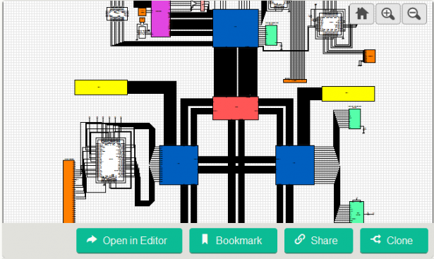
This circuit is designed for dedicated graphic display applications. It shows the basic configuration of personal computer hardware and functions. It is a generic type of a processing unit that handles display and improves image quality. It also manages data transfer from flash drives and other serial devices such as computer mouse and keyboard.
The design is comprised of different parts that serve different functions. The PX1011B-EL1 device is a high-performance, low-power, single-lane PCI Express electrical PHYsical layer (PHY) that handles the protocol and signaling between FPGA and Motherboard. The FPGAs or field-programmable gate arrays serves as the main processors of this designed circuit. It is configured to process data at very fast rate and control bidirectional data buses including I/Os for the display. It has memory interfaces that handle the SRAM, DRAM, and Flash memory. It also has accelerator functions that handle displays and other monitoring applications and fixed peripherals that handle GIGe, USB, CAN, I2C, SD, UART and GPIO. The Static Random Access Memory (SRAM) device is a memory component that is used as a cache memory of FPGA. The Dynamic Random Access Memory (DRAM) stores bits of data in separate capacitor within an integrated circuit. It also serves as the main memory element so that the FPGA’s work will be lessened. The PTN36242L is a dual port SuperSpeed USB 3.0 redriver IC that enhances signal quality by performing receive equalization on the deteriorated input signal followed by transmit de-emphasis maximizing system link performance. The USB microcontroller is a programmable interface chip that is used to integrate USB 2.0 port. The USB 2.0 is provided for longer cable length applications. The PCA24S08A is Electrically Erasable and Programmable Read-Only Memory (EEPROM), which allow you to reprogram the VID/PID for the USB device Identification.
For more detail: Supercomputing Video Card for Personal Computer

