
Summary of Reverse engineering the popular 555 timer chip (CMOS version)
The LMC555 is a low-power CMOS version of the iconic 555 timer, built using MOS transistors instead of bipolar ones. This article details its internal structure via die photos, explaining how N-type and P-type silicon regions, polysilicon wiring, and metal layers form functional blocks like comparators, flip-flops, and current mirrors. It further describes the oscillator operation where external capacitors charge and discharge between 1/3 and 2/3 supply voltage thresholds to generate fixed frequencies.
Parts used in the LMC555 Timer Project:
- LMC555 CMOS integrated circuit
- N-type silicon regions
- P-type silicon regions
- Polysilicon wiring
- Metal interconnect layer
- External capacitor
- External resistors
- Threshold comparator
- Trigger comparator
- Flip-flop
- Discharge transistor
This article explains how the LMC555 timer chip works, from the tiny transistors and resistors on the silicon chip, to the functional units such as comparators and current mirrors that make it work. The popular 555 timer integrated circuit is said to be the world’s best-selling integrated circuit with billions sold since it was designed in 1970 by analog IC wizard Hans Camenzind[1]. The LMC555 is a low-power CMOS version of the 555; instead of the bipolar transistors in the classic 555 (which I described earlier), the CMOS chip is built from low-power MOS transistors. The LMC555 chip can be understood by carefully examining the die photo.
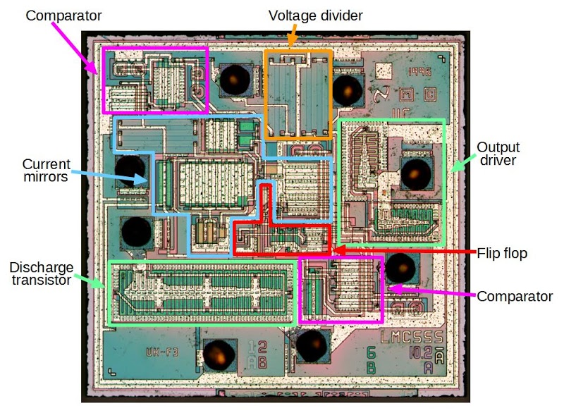
The structure of the integrated circuit
The photo below shows the silicon die of the LMC555 as seen through a microscope, with the main function blocks labeled (photo from Zeptobars). The die is very small, just over 1mm square. The large black circles are connections between the chip and its external pins. A thin layer of metal connects different parts of the chip. This metal is clearly visible in the photo as white lines and regions. The different types of silicon on the chip appear as different colors. Regions of the chip are treated (doped) with impurities to change the electrical properties of the silicon. N-type silicon has an excess of electrons (making it Negative), while P-type silicon lacks electrons (making it Positive). On top of the silicon, polysilicon wiring shows up as other colors. The silicon regions and polysilicon are the building blocks of the chip, forming transistors and resistors, which are connected by the metal layer.
A brief explanation of the 555 timer
The 555 chip is extremely versatile with hundreds of applications from a timer or latch to a voltage-controlled oscillator or modulator. To explain the chip, I will use one of the simplest circuits, an oscillator that cycles on and off at a fixed frequency.
The diagram below illustrates the internal operation of the 555 timer used as an oscillator. An external capacitor is repeatedly charged and discharged to produce the oscillation. Inside the 555 chip, three resistors form a divider generating reference voltages of 1/3 and 2/3 of the supply voltage. The external capacitor will charge and discharge between these limits, producing an oscillation, as shown on the left. In more detail, the capacitor will slowly charge (A) through the external resistors until its voltage hits the 2/3 reference. At that point (B), the threshold (upper) comparator switches the flip flop off turning the output off. This turns on the discharge transistor, slowly discharging the capacitor (C) through the resistor. When the voltage on the capacitor hits the 1/3 reference (D), the trigger (lower) comparator turns on, setting the flip flop and the output on, and the cycle repeats. The values of the resistors and capacitor control the timing, from microseconds to hours.
For more detail: Reverse engineering the popular 555 timer chip (CMOS version)
- What makes the LMC555 different from the classic 555?
The LMC555 uses low-power MOS transistors instead of the bipolar transistors found in the classic version. - How does the 555 timer produce oscillation?
An external capacitor repeatedly charges and discharges between 1/3 and 2/3 of the supply voltage. - What components form the reference voltages inside the chip?
Three resistors inside the chip form a divider that generates reference voltages of 1/3 and 2/3 of the supply voltage. - What happens when the capacitor voltage hits the 2/3 reference?
The threshold comparator switches the flip-flop off, turning the output off and activating the discharge transistor. - What occurs when the capacitor voltage drops to the 1/3 reference?
The trigger comparator turns on, setting the flip-flop and turning the output back on to restart the cycle. - Can the timing duration be adjusted?
Yes, the values of the external resistors and capacitor control the timing range from microseconds to hours. - What are the main building blocks visible on the silicon die?
The silicon regions and polysilicon form transistors and resistors, which are connected by a thin metal layer. - Who designed the original 555 timer?
Hans Camenzind designed the popular 555 timer integrated circuit in 1970.