
Summary of Precision programmable current source uses two ICs
This article describes a programmable current source/sink design combining a precision current source IC (REF200) with a difference amplifier chip (LT1991/5/6). The circuit utilizes tightly matched internal resistor ratios to generate output currents ranging from sink to source configurations, avoiding reliance on absolute resistor tolerances. It specifically addresses compliance voltage limitations and op-amp saturation by paralleling internal feedback resistors.
Parts used in the Programmable Current Source/Sink:
- Precision current source IC (REF200)
- Precision difference amp chips (LT1991/5/6)
- Internal feedback resistor (450 kΩ)
- Parallel connection resistor (450/9 kΩ)
- Negative feedback resistance (45 kΩ)
This Design Idea mates a precision current source IC with precision difference amp chips to create a programmable current source or sink.
The resistor-programmable current source/sink in Figure 1 illustrates the basic topology, taking advantage of tightly matched on-chip resistor ratios instead of relying on absolute tolerances.
he IIN current source gives rise to a reference voltage across Rf at the op-amp inverting input. The same potential is found across the Rf /N resistor, so that an output current of N × IIN will be generated.
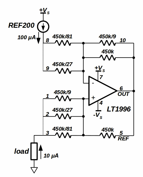
Despite a decreased compliance voltage due to the absence of direct connections to the op-amp inputs, the LT1991/5/6 is used as a single chip current divider. Figure 2 shows an example configuration, with a REF200 as the input current reference. Due to the high value of the internal feedback resistor connected to the op-amp inverting input (450 kΩ), a parallel connection with the 450/9 kΩ resistor is necessary to avoid op-amp output saturation induced by the injected IIN current. The negative feedback resistance is thus equal to 450/10 kΩ, or 45 kΩ.
Given the 450 kΩ positive feedback resistor, N for Figure 2 is 0.1, yielding an output sink current of 10 μA. Different values of the output current can be obtained using the other available internal resistors. If an output source current is needed, reverse the connections to the REF200 IC, and connect it to –VS.
The dotted lines in Figures 2 & 3 illustrate how unused internal resistors can be paralleled to reduce voltage drops in the reference and load paths.
For more detail: Precision programmable current source uses two ICs
-
How does the circuit generate the output current?
The IIN current source creates a reference voltage across Rf, causing an output current of N × IIN to be generated across the Rf /N resistor. -
Why are internal resistor ratios used instead of absolute tolerances?
The design takes advantage of tightly matched on-chip resistor ratios to ensure accuracy without relying on absolute tolerances. -
What causes op-amp output saturation in this configuration?
Saturation is induced by the injected IIN current due to the high value of the internal feedback resistor connected to the op-amp inverting input. -
How is the negative feedback resistance calculated for Figure 2?
A parallel connection between the 450 kΩ internal resistor and the 450/9 kΩ resistor results in a total negative feedback resistance of 45 kΩ. -
What determines the value of N in the example configuration?
Given the 450 kΩ positive feedback resistor, N is determined to be 0.1, yielding an output sink current of 10 μA. -
How can an output source current be achieved instead of a sink?
To obtain an output source current, reverse the connections to the REF200 IC and connect it to -VS. -
What is the purpose of the dotted lines in Figures 2 & 3?
The dotted lines illustrate how unused internal resistors can be paralleled to reduce voltage drops in the reference and load paths.
