Summary of PICKIT 3 MINI
This project streamlined a Pickit 3-compatible programmer/debugger by removing unneeded circuitry for 3.3V PIC32 development. The designer based the simplified schematic on Microchip’s Pickit On-Board, retained essential components (EEPROM, PIC24FJ256GB106 MCU, USB Mini-B, 3.3V regulator), and used voltage dividers and fixed pulls to emulate omitted sensing and switch circuits. A quick PCB layout was produced as a proof of concept intended for inclusion on prototype boards for on-board programming and debugging.
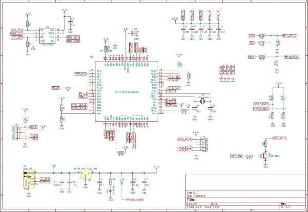
Parts used in the Pickit 3 Mini:
- 25LC256 EEPROM
- PIC24FJ256GB106 microcontroller
- USB Mini-B connector
- 3.3V voltage regulator
- Target MCU programming header
- PICKIT programming header
- Transistor for target MCU master-clear (MCLR) control
- Voltage divider networks for VPP_SENSE and VDD_SENSE
- Voltage divider providing 2.5V reference to PIC pin 16
- Target MCU clock and data lines wiring
Previously, I made a Pickit 3 clone – (See previous Blog Post). It works well, but I have often wondered just how little of its circuitry was needed to program and debug the boards I make. For instance – I primarily use the newer 3.3V PIC32 processors, so I really don’t need the ability to alter the voltage like the standard Pickit 3 can. I also have no real need for programming on the go, or even to provide power to the target MCU to program. Knowing this – I decided to see what I could do to remove the circuitry I didn’t need, yet still have a functioning programmer/debugger.
After a little research and looking at what Microchip had done with their starter kits, I arrived at the following schematic, which is based on their Pickit On-Board:
Here is a link to a PDF of the schematic: PDF Schematic
In the top left of the schematic is the 25LC256 EEPROM. Working our way down we see the main MCU the PIC24FJ256GB106 – and it’s programming header to the left, and below that is the USB Mini-B connector and the 3.3V regulator. Just above that and to the right is the target MCU programming header. To the right of that is a transistor that controls the target MCU master-clear line. Above that are a couple of voltage dividers that mimic the programming and target mcu voltages, and above that are the target MCU clock and Data lines.
This circuit looks to be the same basic underlying Pickit 3 circuit, but with some “faking” of inputs to mimic missing circuitry. For instance – the OTG programming switch would normally be on pin 21, but instead it is simply pulled high as there is no switch to pull it low. VPP_SENSE and VDD_SENSE are simply fed to the PIC by way of voltage dividers, as is the 2.5 volt reference at pin 16.
As it appeared I had everything I needed, I went about laying out the PCB. Since my ultimate goal with this project is to simply include these parts on my prototype development boards so that I can program and debug with an on-board device, I did not spend a lot of time routing the board. It is a quick and dirty that I am using as a proof of concept. If I intended to make these for long term use, I would have spent some time laying it out properly.
Read More: PICKIT 3 MINI
- What was the goal of the Pickit 3 Mini project?
To remove unneeded Pickit 3 circuitry for 3.3V PIC32 development while retaining programming and debugging functionality. - Which MCU is used as the main controller in the design?
The PIC24FJ256GB106 is used as the main MCU. - Is a power supply for the target MCU included in this design?
No, the design does not include providing power to the target MCU; it is intended for use with externally powered targets. - How are VPP_SENSE and VDD_SENSE handled in this simplified circuit?
They are fed to the PIC via voltage divider networks that mimic the original sensing circuitry. - How is the OTG programming switch handled?
Instead of a physical switch, the OTG programming input is simply pulled high since no switch is needed. - What component provides nonvolatile storage in the design?
The 25LC256 EEPROM provides nonvolatile storage. - How is the target MCU master-clear (MCLR) controlled?
A transistor is used to control the target MCU master-clear line. - Does the design include a 2.5V reference and how is it implemented?
Yes, a 2.5V reference is provided to PIC pin 16 using a voltage divider. - What connector is used for USB on the Pickit 3 Mini?
A USB Mini-B connector is used. - Was the PCB layout finalized for production?
No, the PCB was routed quickly as a proof of concept and was not optimized for long-term production use.