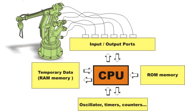
Summary of PIC Microcontrollers – Programming in BASIC
The PIC16F887 is a versatile Microchip microcontroller featuring RISC architecture, 35 instructions, and up to 20 MHz operation. It includes 8K Flash ROM, 256 bytes EEPROM, and 368 bytes RAM across four banks. Key peripherals include a 14-channel ADC, three timers, PWM, USART, MSSP (SPI/I2C), and analog comparators. The article details its memory organization, stack functionality, interrupt system, and Special Function Registers (SFRs) for controlling hardware modules like the A/D converter and communication ports.
Parts used in the PIC16F887 Microcontroller Project:
- PIC16F887 Microcontroller
- PC with programming software
- Electronic programmer device
- Quartz crystal oscillator
- LEDs
- Sensors
- Assembly line components
- mikroBasic PRO compiler
The PIC16F887 is a product of Microchip. It features all the modules that modern microcontrollers normally have. For its low price, wide range of application, high quality and easy availability, it is an ideal solution in applications such as the control of different processes in industry, measurement of different values etc. A list below includes only some of its key features.
THE PIC16F887 BASIC FEATURES
- RISC architecture
- Only 35 instructions to learn
- All single-cycle instructions except branches
- Operating frequency 0-20 MHz
- Precision internal oscillator
- Factory calibrated
- Software selectable frequency range of 8MHz to 31KHz
- Power supply voltage 2.0-5.5V
- Consumption: 220uA (2.0V, 4MHz), 11uA (2.0 V, 32 KHz) 50nA (stand-by mode)
- Power-Saving Sleep Mode
- Brown-out Reset (BOR) with software control option
- 35 input/output pins
- High current source/sink for direct LED drive
- software and individually programmable pull-up resistor
- Interrupt-on-Change pin
- 8K ROM memory in FLASH technology
- Chip can be reprogrammed up to 100.000 times
- In-Circuit Serial Programming Option
- Chip can be programmed even embedded in the target device
- 256 bytes EEPROM memory
- Data can be written more than 1.000.000 times
- 368 bytes RAM memory
- A/D converter:
- 14-channels
- 10-bit resolution
- 3 independent timers/counters
- Watch-dog timer
- Analogue comparator module with
- Two analogue comparators
- Fixed voltage reference (0.6V)
- Programmable on-chip voltage reference
- PWM output steering control
- Enhanced USART module
- Supports RS-485, RS-232 and LIN2.0
- Auto-Baud Detect
- Master Synchronous Serial Port (MSSP)
- supports SPI and I2C mode

- supports SPI and I2C mode
PINOUT DESCRIPTION
Most pins of the PIC16F887 microcontroller are multi-functional. For example, the fifth pin of the microcontroller is marked as RA3/AN3/Vref+/C1IN+ which indicates that it has the following functions:
- RA3 Port PORTA third digital input/output
- AN3 Third analog input
- Vref+ Positive voltage reference
- C1IN+ Comparator C1 positive input
This principle of multifunctionality is commonly applied when designing microcontrollers as it enables the microcontroller package to be much more compact yet not affecting the operation of the microcontroller. Various pin functions cannot be used simultaneously, but can be changed at any point during operation.
The following tables refer to the DIP40 PIC16F887 microcontroller.
CENTRAL PROCESSOR UNIT (CPU)
As any attempt to explain the operation of the CPU in detail would take us too far, we are not going to do it at this stage. Anyway, it is important to point out that the CPU is manufactured in RISC technology as this fact may be crucial when deciding which microcontroller to use.
RISC stands for Reduced Instruction Set Computer, which gives the PIC16F877 two great advantages:
- The CPU is capable of recognizing and executing only 35 simple instructions. By the way, to program other microcontrollers in assembly language it is necessary to know more than 200 instructions by heart.
- The execution time is the same for almost all instructions, and lasts 4 clock cycles. The clock frequency is stabilized by a quartz crystal. The exceptions to the rule are jump and branch instructions the execution time of which is 2 clock cycles. It means that if the microcontroller’s operating frequency is 20MHz, the execution time of each instruction will be 200nS, i.e. the program will execute 5 million instructions per second!
MEMORY
The PIC16F887 features three types of memory: ROM, RAM and EEPROM. Each deserves to be separately discussed here due to their specific functions, features and organization.
ROM
ROM is used to permanently save the program being currently executed. This is why it is often called a ‘program memory’. The PIC16F887 has 8Kb of ROM (8192 locations in total). Since ROM is made with FLASH technology, its contents can be easily changed by providing a special programming voltage (13V).
No further explanations are required as the whole process is performed automatically by means of a special program installed on the PC and a simple electronic device called the programmer.
EEPROM
Similar to the program memory, the content of EEPROM is permanently saved, even when the power goes off. On the other hand, unlike ROM, the contents of EEPROM can be changed during the microcontroller operation. This is why this memory (containing 256 locations) is perfect as a permanent storage for some of the results created and used during the operation.
RAM
This is the third and the most complex type of all microcontroller memory modules. It consists of two parts: general-purpose registers and special-function registers (SFRs). All of them are divided in four memory banks to be explained later in the chapter.
Although both groups of registers are cleared when power goes off and both are manufactured in the same and act in a similar manner, they do not have many things in common when it comes to their functions.
GENERAL-PURPOSE REGISTERS
General-purpose registers are used for storing temporary data and results created during operation. For example, if the purpose of a program is to count something (products on the assembly line, for example), it is necessary to have a register which stands for what in everyday life is called ‘sum’. Since the microcontroller is not creative at all, it is necessary to specify the exact address of some general purpose register and assign it that function. Make sure that the value of this register is incremented by 1 after each product passes through a sensor. This is how a simple program is created.
'In this program section, the variable stored in register sum is incremented every
'time the RB0 input pin is driven high (1)
...
if PORTB.0 = 1 ' Check whether the RB0 pin is driven high
sum = sum + 1  ' If true, the variable value is incremented by 1
end if         ' If false, the program exits the if statement
...
The microcontroller is able to execute this program as it knows what the sum to be incremented is and where it is stored. Similarly, each program variable must be preassigned some of the general-purpose registers.
SPECIAL FUNCTION REGISTERS (SFRS)
Special-function registers also occupy RAM locations, but unlike general-purpose registers, their function is predetermined during the manufacturing process and cannot be changed later. Since their bits are connected to some on-chip modules, such as A/D converter, serial communication module, etc, any change of their contents will directly affect the operation of the microcontroller or at least some of its modules. For example, the ADCON0 register controls the operation of A/D converter. By changing its bits it is determined which port pin is to be configured as a converter input, the start time and speed of conversion. Furthermore, each SFR register has its own name (both registers and their bits), which considerably simplifies the process of program writing. Since high-level programming languages contains a list of all SFR registers with their exact addresses, it is sufficient to specify the name of a register in order to read or change its contents.
Another feature of these memory locations is that they have their names (both registers and their bits), which considerably simplifies the process of writing a program. Since high-level programming languages can use the list of all registers with their exact addresses, it is enough to specify the name of a register in order to read or change its contents.
'In this program section, registers TRISC and PORTC are changed
...
TRISC = 0x00      ' a logic zero (0) is written to register TRISC (all port
                  ' PORTC pins are configured as outputs)
PORTC = %01100011 ' Logic states on all port PORTC pins are being changed
...
RAM BANKS
The RAM is partitioned into four banks. Prior to accessing any register during program write (whether to read or change its contents), it is necessary to select the bank containing it. Two bits of the STATUS register are used for bank selection, which will be discussed later. To make dealing with SFRs as simple as possible, the most commonly used registers have the same address in all banks and therefore can be easily accessed.
It may be difficult to deal with banks when you write a program in assembly language. On the contrary, when you write a program in higher programming languages, such as Basic, and use compilers such as mikroBasic PRO for PIC, it is sufficient to specify the name of a re gister you need. Having this information, the compiler is capable of selecting the appropriate bank as well as to include appropriate instructions into the code during the process of compiling. You have been using only assembly language so far and this is the first time you use the mikroBasic PRO for PIC compiler, isn’t it? This must be a wonderful news then.
STACK
A part of RAM used as stack consists of eight 13-bit registers. Before the microcontroller starts to execute a subroutine (GOSUB instruction) or when an interrupt occurs, the address of the instruction to be executed next is pushed onto the stack, i.e. one of its registers. As a result, the microcontroller knows from where to continue regular program execution when a subroutine or an interrupt execution is complete. The address is cleared after the return to the program and one stack location is thus automatically available for further use.
Note that data is always circularly pushed onto the stack. It means that after the stack has been pushed eight times, the ninth push overwrites the value that was stored with the first push. The tenth push overwrites the second push and so on. Data overwritten in this way is not recoverable. Since the programmer cannot access these registers for write or read and there is no bit to indicate stack overflow or underflow condition, it is necessary to pay special attention to it during program writing.
Let’s do it in mikroBasic…
' When entering an assembly code section inserted in the program, the compiler
' stores data in the currently active RAM bank. It means that in this program
' section, bank selection depends on the SFRs in use. After return to the program
' section written in mikroBasic, the control bits selecting the active bank
'(RP0 and RP1) must return the state they had before the assembly code
' execution. The saveBank auxiliary variable saves the state of these two bits.
saveBank = STATUS and %01100000 ' Save the state of bits RP0 and RP1
' (bits 5 and 6 of the STATUS register)
asm ' Start of assembly sequence
...
... ' Assembly code
...
end asm ' End of assembly sequence
STATUS = STATUS and %10011111 ' Bits RP0 and RP1 return their original state
STATUS = STATUS or saveBank
...
...
INTERRUPT SYSTEM
The first thing to be done by the microcontroller, when an interrupt request arrives, is to execute the current instruction, then to stop the regular program execution. The current program memory address is automatically pushed onto the stack and the default address (predefined by the manufacturer) is written to the program counter. The location from where the program proceeds with execution is called an interrupt vector. For the PIC16F887 microcontroller, the address is 0004h. As seen in figure below, the interrupt vector should be skipped during regular program execution.
A part of the program to be executed when an interrupt request arrives is called an interrupt routine (it is a subroutine in fact). The first instruction of the interrupt routine is located at the interrupt vector. How long will it take to execute the subroutine and what it will be like, depends on the skills of the programmer as well as on the interrupt source itself. Some microcontrollers have a couple of interrupt vectors (every interrupt request has its vector), whereas this microcontroller has only one. This is why the first part of every interrupt routine should be interrupt source detection. When the interrupt source is known and interrupt routine is executed, the microcontroller reaches the RETFIE instruction, pops the address from the stack and proceeds with program execution from where it left off.
MikroBasic recognizes an interrupt routine to be executed by means of the interrupt keyword. The interrupt routine should be written by the user.
sub procedure interrupt ' Interrupt routine
cnt = cnt + 1 ; ' Interrupt causes variable cnt to be incremented by 1
end sub
How to Use SFRs
You have bought the microcontroller and have a great idea how to make use of it… There is a long list of SFRs and their bits. Each of them controls some process within the microcontroller. It really looks like a big control table with a lot of instruments and switches. Now you are concerned about whether you will be able to learn how to use them all? Probably not, but don’t worry because you don’t have to. Powerful devices such as microcontrollers are similar to supermarkets: they offer many things at low prices and it is up to you to choose what you need. Therefore, choose the area you are most interested in and learn only what you have to. When you get a full understanding of hardware operation, study SFRs which are in control of it (there are usually a few of them).
The performance of all devices is controlled by an appropriate control system and the microcontroller is no exception to the rule. One has to be familiar with such systems in order to be able to use devices properly. Of course, we are talking about SFRs where the whole story about programming starts and ends.
CORE SFRs
The following text describes the core SFRs of the PIC16F887 microcontroller. Their bits control different modules within the chip and therefore are described along with processes they are in control of.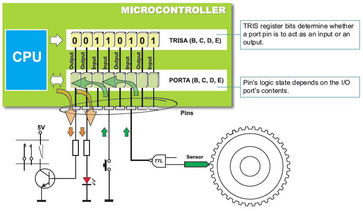
STATUS Register
The STATUS register contains the arithmetic status of data in the W register, reset status and bank select bits for data memory.
- IRP – Bit is used for selecting register bank at indirect addressing.
- 1 – Banks 0 and 1 are active (memory locations 00h-FFh); and
- 0 – Banks 2 and 3 are active (memory locations 100h-1FFh).
- RP1,RP0 – Bits are used for selecting register bank at direct addressing.
| RP1 | RP0 | Active Bank |
|---|---|---|
| 0 | 0 | Bank0 |
| 0 | 1 | Bank1 |
| 1 | 0 | Bank2 |
| 1 | 1 | Bank3 |
- TO – Time-out bit.
- 1 – After power-on, the execution of the
CLRWDTinstruction which resets the watch-dog timer or the SLEEP instruction which sets the microcontroller to the low-consumption mode. - 0 – After the watch-dog timer time-out occurs.
- 1 – After power-on, the execution of the
- PD – Power-down bit.
- 1 – After power-on or the execution of the
CLRWDTinstruction which resets the watch-dog timer. - 0 – After the execution of the
SLEEPinstruction which sets the microcontroller to the low-consumption mode.
- 1 – After power-on or the execution of the
- Z – Zero bit
- 1 – The result of an arithmetic or logic operation is zero.
- 0 – The result of an arithmetic or logic operation is different than zero.
- DC – Digit carry/borrow bit is changed during addition and subtraction if an ‘overflow’ or a ‘borrow’ of the result occurs.
- 1 – A carry-out from the 4th low-order bit of the result has occurred.
- 0 – No carry-out from the 4th low-order bit of the result has occurred.
- C – Carry/Borrow bit is changed during addition and subtraction if an ‘overflow’ or a ‘borrow’ of the result occurs, i.e. if the result is greater than 255 or less than 0.
- 1 – A carry-out from the most significant bit (MSB) of the result has occurred.
- 0 – No carry-out from the most significant bit (MSB) of the result has occurred.
For more detail: PIC Microcontrollers – Programming in BASIC
- What is the operating frequency range of the PIC16F887?
The operating frequency ranges from 0 to 20 MHz. - How many instructions must be learned to program this microcontroller?
Only 35 instructions need to be learned as it uses RISC architecture. - Can the ROM memory be reprogrammed?
Yes, the chip can be reprogrammed up to 100,000 times using FLASH technology. - Does the PIC16F887 support multiple serial communication protocols?
Yes, the Enhanced USART module supports RS-485, RS-232, and LIN2.0, while MSSP supports SPI and I2C. - How many analog input channels are available on the A/D converter?
The A/D converter features 14 channels with 10-bit resolution. - What happens when an interrupt request arrives at the microcontroller?
The current instruction finishes, the address is pushed onto the stack, and execution jumps to the interrupt vector at address 0004h. - How is the RAM organized in the PIC16F887?
The RAM is partitioned into four banks containing general-purpose registers and special-function registers. - What is the capacity of the EEPROM memory?
The microcontroller has 256 bytes of EEPROM memory that can be written more than 1,000,000 times. - Can the microcontroller operate in a low-consumption mode?
Yes, it features a Power-Saving Sleep Mode and consumes 50nA in stand-by mode. - How does the compiler handle bank selection in mikroBasic PRO?
The compiler automatically selects the appropriate bank and includes necessary instructions during compilation.