Summary of Making a PCB Business Card
The author adapted an earlier PCB ruler concept into a PCB business card showing component footprints, scales, braille phone number, and Morse-coded website. Manufactured cheaply by Dirt Cheap PCB, the cards look good though silkscreen can fuzz and AWG holes were plated unintentionally; maker code placement suggested swapping layers next time.
Parts used in the PCB Business Card:
- PCB substrate (custom board)
- Silkscreen printing
- AWG drill holes
- Braille dots (silkscreen or solder mask/raised features)
- Morse code dots and dashes (silkscreen)
- Component footprints (various common PCB component outlines)
- Plated through holes (for AWG holes, as produced)
Many of you may have seen the Adafruit PCB ruler (also used by the awesome Voltera).
The design was actually adapted from my own design back in University!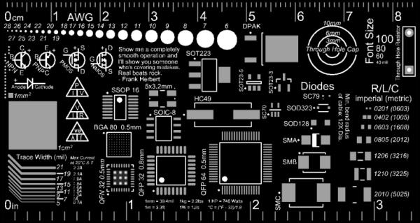
To improve on the original idea, I have created a reference business card.
Here is a computer render of the design:
PS. The dots on the front are the phone number in braille, the dots and dashes are Morse for the website, cause who doesn’t surf the web by Morse?
I wanted to show every common component I could think of, and how they relate. Often when zoomed all the way into a digital design, you can lose track of what 5 mils really means. It is TINY!
Here is what it looks like in real life:
The PCBs were made by Dirt Cheap PCB and overall look pretty good. The silkscreen can be a bit fuzzy or misaligned, but at ~2$ per card, this is great! The slight annoyance is that they plated the AWG holes, even though this was not specified.
Another tip: You can see the maker’s code on the front of the card (white text below the braille). Manufacturers will often put this on the “back” side of your design (bottom layer) so for next time, I will swap the layers to place the mark on the less pretty back.
For more detail: Making a PCB Business Card
- What inspired the PCB business card design?
The design was adapted from the author’s earlier PCB ruler concept used by Adafruit and Voltera. - What extra information is encoded on the card?
The front includes a braille phone number and Morse code dots and dashes for the website. - Who manufactured the PCBs?
The PCBs were made by Dirt Cheap PCB. - How is the silkscreen quality described?
The silkscreen can be a bit fuzzy or misaligned. - Were the AWG holes produced as expected?
The manufacturer plated the AWG holes even though plating was not specified. - What will the author change for future boards regarding maker marks?
The author will swap layers to place the maker’s code on the less pretty back side next time. - Why include many component footprints on the card?
To show every common component and illustrate relative sizes so designers don’t lose perspective at high zoom.