Summary of Introduction to Microchip PIC Assembler Language – Part 2
This article explains the efficient yet challenging nature of Microchip PIC assembler, highlighting its unique bit-test instructions compared to other microcontrollers. It details the standard program skeleton for the PIC12F683, covering configuration bits, register banking (BANK 0 and BANK 1), and essential initialization routines using specific MPASM directives and commands like BSF, BCF, MOVW, and CLRF.
Parts used in the PIC12F683 Assembler Project:
- PIC12F683 microcontroller
- MPASM Compiler
- p12F683.INC file
- Configuration bits register
- Delay1 variable
- Delay2 variable
- STATUS register
- OSCCON register
- TRISIO register
- ANSEL register
- WREG accumulator
With only 35 instructions to learn the Microchip PIC microcontroller assembler language is considered very efficient and easy to learn; you will not find such as Atmel AVR microcontroller CP (compare) and BRNE (branch if not equal) or BRGE (branch if greater or equal) on the PIC microcontroller assembler language dialect, instead it’s just provide us with a very simple bit test and skip one line instruction. This fact is what makes programming the PIC microcontroller assembler language become very interesting and challenging, therefore although is easy to learn but for sure you will need a lot of flying time in order to code the PIC microcontroller efficiently.
The PIC Assembler Program Skeleton:
Continuing our lesson with the 8-bit, 8 pins midrange Microchip PIC12F683 microcontroller, I will start with the typical PIC microcontroller assembler program skeleton bellow:
The first part is the program comment; it’s always a good practice to put a comment to your program e.g. name, version, description, etc. All lines begin with ; sign is consider a comment to the MPASM (Microchip PIC Assembler) compiler.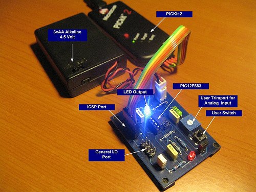
The second part is the #include <p12F683.INC> MPASM compiler directive which tell the compiler to include the PIC12F683.INC file definition which exist in the c:\Program Files\Microchip\MPASM Suite directory (MPLAB IDE v8.00 default installation). This include file contain the standard PIC microcontroller physical address to the equivalent naming convention; for example instead of using the address 0x05 (5 hex) for general purpose I/O, we could use GPIO which is easier to remember.
The third part is the Microchip PIC microcontroller configuration bits register; this register is start at address 2007 on the PIC12F683 microcontroller and has 14 bits long. This register is one of the unique features of the PIC Microcontroller compared to other microcontroller, the PIC configuration bits could be configured on every startup of the program.
The configuration bits register is used to set how the PIC microcontroller work such as choosing the internal or external clock, using the master clear or not, etc. When programmed these bits will be read as “0“; for un-programmed these bits will be read as “1“. The following table shows the configuration bit used in our Hello World assembler program.
The complete description of this configuration bit could be found at page 84 on the Microchip PIC12F63 microcontroller datasheet; therefore by using the AND operator to the entire PIC MPASM configuration bit definition value we could configure the desire configuration bit register value or we could simply using just the bit value as shown on this following table:
Base on the configuration bit table shown above, we could set the PIC12F683 microcontroller configuration bit directly and this will give you the same result as the above program example:
The fourth part is the MPASM CBLOK 0x20 and closed with ENDC directive; which tell the MPASM compiler to map the Delay1 and Delay2 variables to the 8-bit general purpose registers which start at the address 0x20 on the PIC12F683 microcontroller address BANK 0; the Delay1 will be mapped to the general purpose register at the address 0x20 and the Delay2 will be mapped to the general purpose register at the address 0x21. The following picture show all the Microchip PIC12F683 microcontroller registers address which split into 2 groups named BANK 0 and BANK 1.
One of the unique things about the PIC microcontroller registers address comparing to other microcontroller that the address is not in one continues memory but its being split into two BANKS (groups); this mean we have to switch back and forth between the BANK addresses to access the desire register. For example if we want to access the register TRISIO, we have to switch to the BANK 1 before we could access it and switch back to the BANK 0 in order to access the GPIO register.
To make it easier to understand you could consider the BANK 0 and BANK 1 are like the DIRECTORIES in your computer file system, so if you want to access the TRISIO register (just like a file reside in your directory), you have to change the directory first to the BANK 1 before you could use this register and change directory back to the BANK 0 to access the GPIO register. If you notice some of the registers such as the STATUS register is shared or appeared to the both BANKS; this mean it doesn’t matter which BANK you are right now, you could always access this register. This is the same principal as the LINK file on the UNIX/Linux operating system file system, that one physical file could appear on many directories using just the link name.
The fifth part is the ORIGINATE (org) MPASM compiler directive that tell the MPASM compiler that your code is start at the address 0x0000 of the PIC microcontroller flash memory.
The sixth part is where you put your PIC assembler program code; this code could consist of main program and the subroutine or function.
The last part is the end MPASM compiler directive that tell the MPASM compiler that your code is end here and it’s a good practice to put the EOF (end of file) comment mark in your program so whenever you cut and paste the program to the other project you could make sure that all the codes is being copied until the EOF mark.
Inside the HelloWorld Program
Now we will walk through the program codes, first thing I will explain the initialization routine to the PIC12F683 microcontroller; in this initialization routine you will learn the top five of the 35 PIC12F683 microcontroller assembler instructions that you will certainly use in every project. Before we start make sure you have the PIC12F683 datasheet near you and open the page 101 on the Instruction Set Summary.
Start:
     bsf    STATUS,RP0    ; Select Registers at Bank 1
     movlw  0x70
     movwf  OSCCON        ; Set the internal clock speed to 8 Mhz
     clrf   TRISIO        ; Set all General Purpose I/O to output
     clrf   ANSEL         ; Make all ports as digital I/O
     bcf    STATUS,RP0    ; Back to Registers at Bank 0
The first thing in our initialization routine is to set the internal clock speed which can be controlled in the oscillator control register or OSCCON at BANK 1, we decide to run the PIC12F683 microcontroller with the maximum internal clock speed of 8 Mhz as shown on the OSCCON register bellow:
By making the internal oscillator selection bits IRCF2=1, IRCF1=1 and IRCF0=1 on the OSCCON register we select the 8 Mhz of internal oscillator frequency, this could be written as the following C program:
But in the PIC assembler code, before we could use the OSCCON register we have to change to the BANK 1, since the default BANK when the PIC microcontroller power up is in the BANK 0; How to instruct the PIC microcontroller to change to the BANK 1; this could be done by setting the bank selection register bits RP1 and RP0 on the STATUS register.
Because the PIC12F683 microcontroller only have two BANKS, then the RP1 bit is not use; but for some PIC microcontroller families such as PIC16F690 or PIC16F886 families have four BANK addresses; therefore for this PIC microcontroller families both RP1 and RP0 bits are used to select the BANK addresses. By setting the bit RP0 to logical “1” we instruct the PIC12F683 microcontroller to change to the BANK 1 and by clearing the bit RPO to logical “0“, we instruct the PIC12F683 microcontroller to change back to the BANK 0 (default). The famous PIC set and clear bit oriented file register operation could be used to achieve this task.
bsf f,b -> Bit Set f: Register Address (0x00 to 0x7F) and b: is the bit address
bcf f,b -> Bit Clear f: Register Address (0x00 to 0x7F) and b: is the bit address
bsf STATUS,RP0 ; Select Registers at Bank 1
This instruction will simply tell the PIC microcontroller to SET the RPO bit (the fifth bit) on the STATUS (address 0x03) register and to CLEAR the RPO bit on the STATUS register we use this command bellow:
bcf STATUS,RP0 ; Back to Registers at Bank 0
As you seen from time to time we have to change the BANK address in order to access the desired registers and we always use the STATUS register to achieve this task; therefore now you understand why the PIC microcontroller shared this STATUS register through all the PIC’s BANK addresses, so you could always access this important register regardless of the BANK address you are in right now.
After we change to the BANK 1 in order to assign the 0x70 value into the OSCCON register, we have to put first the value in the PIC microcontroller 8-bit accumulator register named WREG (working register) and then move this accumulator value into the OSCCON register. Again the two most used PIC assembler instructions will be used to achieve these tasks:
movlw k -> Move literal (constant) to WREG, k is the 8-bit constant
movwf f -> Move the WREG value to f: Register Address (0x00 to 0x7F)
movlw  0x70
movwf  OSCCON        ; Set the internal clock speed to 8 Mhz
The tri-state register TRISIO and the analog selection register ANSEL located at BANK 1 are used to set the PIC microcontroller I/O port behavior:
For more detail: Introduction to Microchip PIC Assembler Language – Part 2
- How does the PIC assembler differ from Atmel AVR regarding branch instructions?
PIC assembler uses simple bit test and skip instructions instead of complex compare and branch commands like BRNE or BRGE. - What is the purpose of the #include p12F683.INC directive?
It tells the compiler to include the file definition containing physical address naming conventions like GPIO. - Where are the Delay1 and Delay2 variables mapped in memory?
They are mapped to general purpose registers at addresses 0x20 and 0x21 in BANK 0. - Why must a programmer switch between BANK 0 and BANK 1?
The register addresses are split into two groups, requiring a directory change to access specific registers like TRISIO or GPIO. - Which instruction sets the internal clock speed to 8 MHz?
The combination of moving 0x70 into the OSCCON register after switching to BANK 1 sets the speed to 8 MHz. - How do you select the registers at Bank 1 using the STATUS register?
You use the bsf instruction on the RP0 bit of the STATUS register. - What happens when configuration bits are programmed versus un-programmed?
Programmed bits read as 0, while un-programmed bits read as 1. - Which register is shared across both BANK 0 and BANK 1?
The STATUS register is shared, allowing access regardless of the current bank selection. - What is the function of the ORIGINATE directive in the code?
It tells the compiler that the code starts at address 0x0000 in the flash memory. - What is the default bank state when the PIC microcontroller powers up?
The default bank is BANK 0.