This is a brief review of the capabilities and ease of use of three of the most interesting, innovative and downright disruptive web-based EDA tools:
- EasyEDA
- Upverter
- Autodesk 123D Circuits (formerly Circuits.io)
The same simple astable multivibrator circuit is entered into each tool and the design process followed through simulation (where offered), to PCB layout and Gerber download.
For all of the products reviewed, there’s no need to install any software. They all run in any HTML5 capable, standards compliant web browser. The one limitation is that they are not really designed for use on touch screen platforms such as iPads, Tablets and Smartphones. This is partly because of the screen size limitation (you can’t seriously expect to be able to draw detailed schematics or do PCB layout on anything less than about a 14 inch screen!) but particularly for Upverter and EasyEDA, because they make extensive use of keyboard shortcuts or “Hotkeys” to speed up your work and increase productivity.
EasyEDA
That is a very different deal from that offered by most EDA suppliers, web-based on not.
Working in EasyEDA
Work in EasyEDA is organised in Projects. Projects can be created by clicking on the +New Project button in the upper right corner of the main website pages or from within the Editor window. Projects can be shared with specific colleagues or made public and the visible content controlled by clicking on the Project folder in the left hand Navigation panel of the Editor window and selecting Modify. This takes the user to the Project edit page which can also be reached via My Projects under the user drop down menu options the +New Project button.
Schematics in EasyEDA
EasyEDA can create highly professional looking schematics.
EasyEDA has some simple but powerful drawing capabilities, so users can create their own symbols and footprints either by copying existing ones into My Parts then editing and saving them or by drawing them from scratch. It is possible to keep private symbols and footprints by drawing them in schematic and PCB sheets in a private project but otherwise, all symbols and footprints are public and users can earn points towards allowing them more private projects by contributing high quality, well documented, symbol and footprints.
There is also a Symbol Wizard to quickly draw new symbols for DIP, QFP and SIP
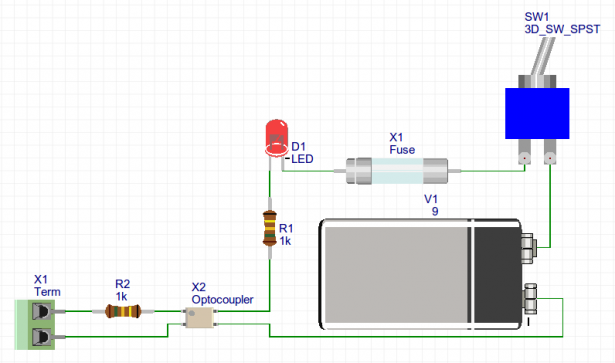
A feature of EasyEDA is that as well as extensive libraries of the usual simple “2D” graphical schematic symbols, it has a library of drawn “3D” component symbols, i.e. symbols that look like the physical components that they represent. So, schematics can be built like this:
For more detail: How to Build PCB Online using Web Based EDA Tools

