Summary of GRAPHENE ENERGY HARVESTING CHIPS CLOSER TO AVAILABILITY
NTS Innovations and the University of Arkansas developed a graphene energy harvesting (GEH) circuit on a silicon wafer that converts ambient nanoscale graphene oscillations into usable power. The GEH device is robust across environments—including space, atmosphere, and deep ocean—limited mainly by its packaging. The technology uses standard semiconductor fabrication, enabling cost-effective mass production. First-generation GEH chips target 10 mW output with a 12 x 12 x 3 mm chip size; the project is moving into prototyping and commercial optimization.
Parts used in the GEH Project:
- Freestanding graphene
- Silicon wafer
- Energy harvesting circuit
- Semiconductor manufacturing processes (common fabrication techniques)
- Packaging (environmental containment)
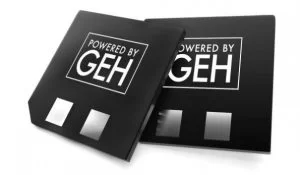
- GEH chip (12 x 12 x 3 mm first-generation design)
Nanotechnology company NTS Innovations says it has achieved a major milestone in its development of a graphene energy harvesting (GEH) clean energy source that can operate in any environment.
GEH is the act of harvesting energy at the nanoscale level from the naturally occurring oscillations in graphene. Freestanding graphene converts ambient energy into mechanical energy in the form of ripple fluctuations, much like waves on the ocean, says the company. Now, in partnership with the University of Arkansas, the company says it has completed the development of its energy harvesting circuit on a silicon wafer.
GEH is a nanoscale device on a semiconductor wafer,” says Preston Carter, Chief Technology Officer at NTS Innovations. “The technology itself varies slightly with temperature but is otherwise robust in all environments. GEH can generate power in outer space and aerospace environments, GEH will work anywhere on Earth, and will continue to work deep in the ocean. The only environmental limitations to GEH will be the packaging used to contain it.
With the development of an energy harvesting circuit complete, the company says it is now moving on to prototypes and optimization for commercial applications. GEH chips are made with common semiconductor manufacturing techniques, making them cost-effective, scalable, and easy to mass produce. The first generation GEH chip is targeted for 10 mW (milliwatts) with a chip size of 12 x 12 x 3 mm.
Read more: GRAPHENE ENERGY HARVESTING CHIPS CLOSER TO AVAILABILITY
- What is GEH?
GEH is graphene energy harvesting, which captures nanoscale ambient oscillations in freestanding graphene and converts them into mechanical and electrical energy. - Can GEH work in space?
Yes; the company states GEH can generate power in outer space and aerospace environments. - Will GEH work underwater?
Yes; GEH will continue to work deep in the ocean, with environmental limits depending on packaging. - What limits GEH operation in environments?
The primary environmental limitation is the packaging used to contain the GEH device. - What power output is the first-generation GEH chip targeted for?
The first-generation GEH chip is targeted for 10 mW. - What is the size of the first-generation GEH chip?
The first-generation GEH chip size is 12 x 12 x 3 mm. - Are GEH chips scalable and cost-effective to produce?
Yes; GEH chips are made with common semiconductor manufacturing techniques, making them cost-effective and scalable. - What is the current development stage of GEH?
The energy harvesting circuit development is complete, and the project is moving to prototypes and optimization for commercial applications.