Getting ready
You’ll need the follow hardware for this lab.
- Breadboard — large or medium
- Microstick
- Two resistors — 330 to 470 Ω
- Two LED’s
- Two push-down switches
- A small amount of wire
Microchip references
- PIC24HJ32GP302/304, PIC24HJ64GPX02/X04 and PIC24HJ128GPX02/X04 datasheet
- PIC24H Family Reference Manual
Pin I/O and the special function registers
On the PIC microcontroller there are a few special function registers (SFR’s) that are used for pin I/O. Some of these registers read and write the pins. Others configure the pins.
Most pins of the chip can be configured for several different modes of operation. Configuration is done by setting bits within special file registers dedicated to pin I/O configuration.
For right now we are going to look at a small subset of the many functions that can be performed using the pins of the PIC microcontroller. Because this subset is adequate to get us through the first few labs, we’re going to pretend that the pins are limited to the following characteristics during this lab.
Digital or Analog
Most, but not all, pins can be used as either digital or analog interfaces. When used for digital I/O, they interpret 0 v as 0 and 3.3 v as 1. When used for analog input, a 16-bit value giving the input voltage level at a pin is provided by the chip. Analog output is a much more complex and depends on PWM (Pulse Width Modulation), a concept that will be introduced in a this lab and discussed more fully in a future lab.
The AD1PCFG register is a register used to configure each pin as digital or analog. By default, pins are analog.
Input or Output
A digital pin can be used for either input or output. By default, digital pins are set for output when the pin is configured for digital I/O using AD1PCFG.
The input or output setting is controlled using the TRISA and TRISB registers. Often this pair is called the TRISx registers. “TRIS” is an abbreviation for TRI-STATE®, a registered trademark of National Semiconductor.
Microchip recommends that unused pins be set to digital output with low written to the pin. This is something we will do in our labs.
The reason why there are two TRISx registers and only one AD1PCFG is that there are 12 pins that go do both analog and digital but 21 that do digital.
Change notification
Pins can be set to interrupt the processor when an input to the chip is changed by an external circuit. This allows the chip to “sleep” to conserve power and plays a significant role in reducing battery life in consumer devices.
Change notification is enabled using the CNEN1 and CNEN2 registers.
Weak pull-ups
“Weak” pull-ups can be enabled on pins supporting change notification. When this is done, an input pin reads as 1 when no external voltage source is “driving” the line connected to the pin. To avoid the cost of an external resistor, weak pull-ups are often used when pins are directly connected to push-button switches. The PIC documentation states that weak pull-ups should be disabled when a pin is used for digital output.
Pull-ups are turned on using the CNPU1 and CNPU2 registers.
Open-drain
Some digital output pins can be set to “drain” their lines. An open-drain pin can “sink” current on a output line until 0 v is reached or it can allow the output to “float” to an externally set value.
Open drain is enabled using the ODCA and ODCB registers; however, the drain is switched on and off using the TRISx registers.
Reading a digital pin
The values of the digital input pins are read using the PORTA or PORTB registers. Do not write to these registers while working on this lab.
Writing to a digital pin
Digital output pins are written using the LATA or LATB latch registers. The LATx registers store the output values that are being written to the external world. It is similar to a D-latch.
If a pin is configured for input, the LATx and PORTx registers can differ. Also, it can take a few microseconds for values written to the LATx register to be reflected in the PORTx registers.
More references
Here are the numbers of some pages from the PIC24HJ32GP302/304, PIC24HJ64GPX02/X04 and PIC24HJ128GPX02/X04 datasheet that provide more information about Pin I/O.
- Page 3 — pinout of the PIC24HJ64GP502
- Page 31 — Table 4-2 and 4-2,
CNENxandCNPUxregisters - Page 36 — Table 4-14,
AD1PCFGLregister - Page 44 — Table 4-27, registers for
PORTApins - Page 45 — Table 4-29, registers for
PORTBpins
The downside of multiple usage
Unfortunately, a single physical pin has several names, each reflecting a potential function. For example, physical pin 6 corresponds to analog pin 4 (AN4), change notification pin 6 (C6), and port B pin 2 (RB2). So, if you are using physical pin 6 as an digital input with an internal pull-up; you set bit 4 of AD1PCFGL, clear bit 6 of CNEN, set bit 6 of CNPU1, and set bit 2 of TRISB.
In assembly language this would be
          bset      AD1PCFGL,#PCFG4        ; Set for digital
          bclr      CNEN1,#CN6IE           ; Disable change notification enable
          bset      CNPU1,#CN6PUE          ; Enable change notification pull-up
          bset      TRISB,#TRISB2          ; Set for input
C is a little less verbose.
    _PCFG4 = 1 ;           // Set for digital
    _CN6IE = 0 ;           // Disable change notification enable
    _CN6PUE = 1 ;          // Enable change notification pull-up
    _TRISB2 = 1 ;          // Set for input
Since many pins are configured similarly, it’s easier to set all the bits of a configuration register in a single assignment. We’ll do this is our starter code.
Back to the breadboard
We are going to complete this lab using a Microstick containing a PIC24HJ64GP502 chip. The Microstick allows access to almost all pins of the PIC24HJ64GP502; however, the regulated 3.3 v power supply is not available for external use. If you breadboard needs 3.3 v, you’ll need to include your own voltage regulator. Today we won’t need 3.3 v, so you can remove your voltage regulator if it is in the way.
In this lab your chip will use to two push-down switches for input and two LED’s as output. The switches will be connected to pins 6 (RB2) and 7 (RB3) of the Microstick and the LED’s will be connected, through resistors, to pins 23 (RB12) and 24 (RB13).
Microstick meets breadboard
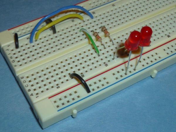
Go ahead and carefully place your Microstick on the breadboard. The pins on the Microstick are fragile, so do not insert the Microstick until you are certain it is properly aligned. Arrange it so that pin 1 of the Microstick is in row 1 of your breadboard. This means that your Microstick will be occupying rows 1 to 14 of your breadboard and the USB interface of the Microstick will be hanging off the board.
Now you need to wire the ground pins of the Microstick to the ground rails of the breadboard. This means running black wires from pins 8, 19, and 27 of your Microstick to the breadboard grounding rails. Pin 8 will be on the a to e side of row 8; pin 19, on the f to j side of row 10; and pin 27, on the f to j side of row 2. On the a to e side of the breadboard, the pin and row numbers are the same. On the f to j side, the sum of the pin and row numbers are 29.
Next build two little subcircuits for your LED’s. In each case the LED connects to the ground rail at its cathode and to a 330 or 470 Ω resistor at its anode. This leaves one unconnected end for each resistor. Connect one resistor to pin 23 (RB12) of the Microstick and connect the other to pin 24 (RB13).
You must use black wires to connect to ground.
Let’s do one more thing. Run a brightly colored wire between the two halves of row 15. The purpose of this wire is to make it difficult for you to place the Microstick in the wrong position on the breadboard.

Programming the Microstick
Connect the Microstick to your computer using the USB cable. Do not place the Microstick on the breadboard yet. We don’t know what program the chip was running last term and can’t be sure that this Microstick and breadboard combination will not produce smoke. (We really know that this particular breadboard is safe for the Microstick, but we don’t want to create bad habits.)
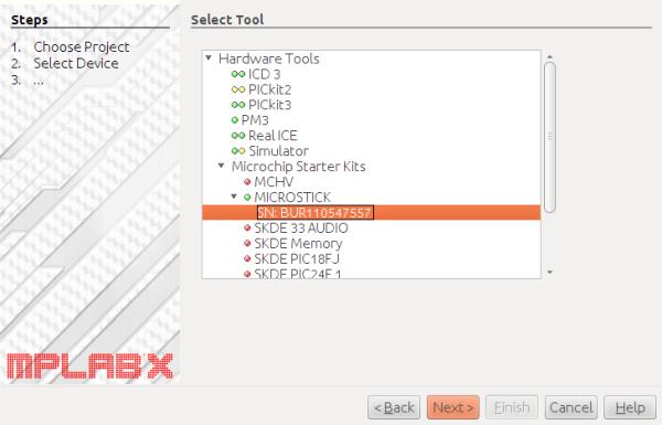
Start MPLABX and create a project just like you have done in recent labs. However when it comes time to choose the hardware device, select your Microstick. You’ll see a different serial number than the one shown in the screen capture below.

The first run
Add the following assembly language program to your project.
include  "xc.inc"
          config    FWDT, FWDTEN_OFF       ; Turn off watch dog timer
          .global   __reset
          .text

__reset:
          mov       #__SP_init,W15         ; Initialize stack
          mov       #__SPLIM_init,W0
          mov       W0,SPLIM

;; Pins used in project
;; Output pins
;; Pin 23 on PIC24HJ64GP502  --  AN12 /         RP12 / CN14 / RB12
;; Pin 24 on PIC24HJ64GP502  --  AN11 /         RP13 / CN13 / RB13

;; All pins of the configuration register are initialized.
          setm      AD1PCFGL               ; Set all pins for digital
          clr       CNEN1                  ; Disable change notification
          clr       CNEN2
          clr       CNPU1                  ; Disable weak pullup
          clr       CNPU2
          clr       ODCA                   ; Disable open drain
          clr       ODCB
          clr       TRISA                  ; Set all pins for output
          clr       TRISB

EndLoop:
          bra       EndLoop

          .end
Build the program to make sure there are no assembler errors. Then use the Make and Program Device icon to program your PIC processor. You should get the message Programming completed if this works.
Now slowly place your PIC into the breadboard. Remember that the pins on the Microstick are fragile, so be careful. This program does nothing except set its pins to be digital outputs, so your LED’s should remain off.
To turn on an LED, add the single statement below before the EndLoop label. Now reprogram your chip.
bset LATB,#LATB13
If you get one LED turn to on, add an additional PIC instruction to light up the other.
Now, replace these two instructions with another two:
          mov       #((1<<LATB13)|(1<<LATB12)),W0
          mov       WREG,LATB
Think about that #((1<<LATB13)|(1<<LATB12)). Be sure you understand how this expression turns on the appropriate bits in the latch. (Hint, LATB13 and LATB12 have been defined as the integers 13 and 12.) Oddly enough, this is the preferred way to set latch bits because the bset instruction reads the existing latch and then writes back an updated copy. The bset is a tiny bit slower than the mov and can cause glitches in the output.
Show the instructor you have turned on the lights.
A little action
Let’s make our project a little flashier. Start by placing the following PIC assembly subroutine in your program, right before the __reset label.
;; A little routine to waste W0*W0*k microseconds
spin:     mov       W0,W7
1:        mov       W7,W3
2:        dec       W3,W3
          bra       nz,2b
          dec       W0,W0
          bra       nz,1b
          return
Don’t worry that this routine blocks the path to __reset. The PIC always starts at __reset. Notice the use of numeric labels such as 1 and 2. This are common in contemporary assemblers. When the assembler sees 1b as the target of a branch, it assumes you are talking about the first numeric label 1 it will encounter as it looks backwards in the program. There is also an “f” for looking forward.
The only thing this subroutine does is waste time in a doubly-nested loop. Modify your program so that it implements the following pseudo-code after the configuration registers are set. There must be two calls to spin in this loop.
    while (1) {
       in LATB turn LATB13 on and LATB12 off
       waste some time ;
       in LATB turn LATB12 on and LATB13 off
       waste some time ;
    }
Use the PIC instruction “rcall spin” to invoke the time wasting subroutine. Set the parameter W0 before each call. The value 1000 worked for me.
Once you have the LED flashing, modify the values used to set the spin time. First, make the LED’s blink very slowly. Then, make LED’s blink so quickly that your eyes cannot tell that the LED is flashing on and off. Finally, set the spin times so that both the LED’s appear to be constantly on but one is noticeably dimmer than the other. This is an example of pulse width modulation (PWM), turning a digital output off and on so quickly that it looks like an analog signal. PWM is used to control motors, and speakers are just motors for moving air.
Show the instructor you have dimmed the lights.
Goodbye to assembly language
Let’s try this again, but this time in C. Create a new project with the same properties, but this time add a C Main File to your project. Delete the initial contents for your C program and replace it with the following C code.
#pragma config FWDTEN=OFF  // Turn off watch dog timer

#include <xc.h>

#include <stdlib.h>
#include <stdint.h>

/*
    Pins used in project
    Output pins
    Pin 23 on PIC24HJ64GP502  --  AN12 /         RP12 / CN14 / RB12
    Pin 24 on PIC24HJ64GP502  --  AN11 /         RP13 / CN13 / RB13
 */

int main(void) {

    AD1PCFGL = 0xFFFF ;    // Set all pins for digital
    CNEN1 = 0 ;            // Disable change notification
    CNEN2 = 0 ;
    CNPU1 = 0 ;            // Disable weak pullup
    CNPU2 = 0 ;
    ODCA = 0 ;             // Disable open drain
    ODCB = 0 ;
    TRISA = 0 ;            // Set all pins for output
    TRISB = 0 ;

    return (EXIT_SUCCESS);
}
You should notice a lot of similarity between this C program and the earlier assembly language program. In C on the PIC, PIC special file registers can be accessed through variable names loaded from the xc.h include file. Through the magic of C’s preprocessor and bit fields, it is also possible to access individual bits of registers. This is seen in the following example of two ways to change bits in a latch register.
        _LATB13 = 1 ;
        LATB = 1 << _LATB_LATB13_POSITION ;
Go ahead and program the device using this C code. You should notice that the LED’s are off. To restore the flash, start by adding the following spin function to your program. (Put it before main.)
void spin(uint16_t loop) {
    uint16_t i, j ;
    for (i=0; i<loop; ++i) {
        for (j = 0; j<loop; ++j) {
        }
    }
}
Now put a forever loop in your program, similar to the one you wrote in the assembly language program, and flash the LED’s.
Prove that C can LED.
Adding inputs
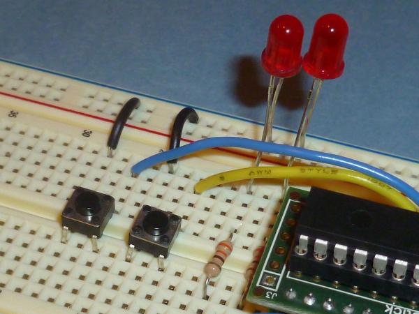
In the next part of the lab, we give the circuit some input. Disconnect the USB cable to the Microstick and place two push-button switches on the breadboard. Connect one side of each switch to the ground rail. Then connect the other side of one switch to pin 6 (RB2). With the other switch, make a similar connection to pin 7 (RB3).
Be very careful in connecting the switches. The switches have four legs. The four legs are really two pairs of always-connected legs on the longer sides of the switch. The pairs are connected when the switch is pushed.
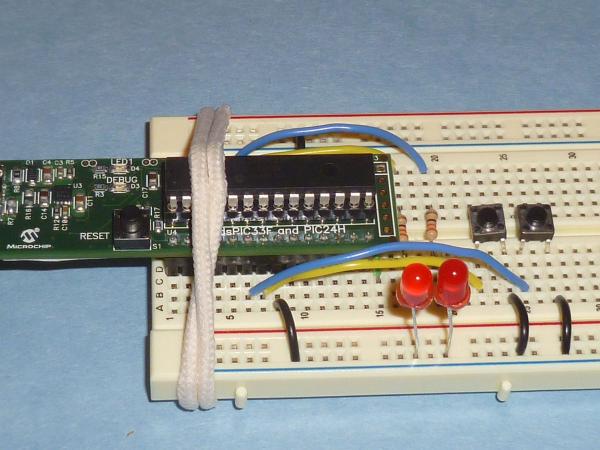
Make sure your breadboard and Microstick configuration matches the following picture. Then make sure your neighbor’s breadboard matches the picture.
Notice the use of hair accessories to hold the Microstick in the breadboard. You are not required to use these, but you are encouraged to use a strong rubber band. This keeps the Microstick from falling off the breadboard.


Plug the USB cable back into the Microstick. The LED’s should start flashing again. You are still running your old program.
A program that reads pins
Now create a third MPLABX project. This time start with the following C program.
#pragma config FWDTEN=OFF  // Turn off watch dog timer

#include <xc.h>

#include <stdlib.h>
#include <stdint.h>

/*
    Pins used in project
    Input pins
    Pin  6 on PIC24HJ64GP502  --   AN4 / C1IN- /  RP2 /  CN6 /  RB2
    Pin  7 on PIC24HJ64GP502  --   AN5 / C1IN+ /  RP3 /  CN7 /  RB3
    Output pins
    Pin 23 on PIC24HJ64GP502  --  AN12 /         RP12 / CN14 / RB12
    Pin 24 on PIC24HJ64GP502  --  AN11 /         RP13 / CN13 / RB13
 */

int main(void) {

    AD1PCFGL = 0xFFFF ;    // Set all for digital
    CNEN1 = 0 ;            // Disable change notification
    CNEN2 = 0 ;
    CNPU1 = (1<<_CNPU1_CN7PUE_POSITION) | (1<<_CNPU1_CN6PUE_POSITION) ;
    CNPU2 = 0 ;            // Disable weak pullup except for RB2 and RB3
    ODCA = 0 ;             // Disable open drain
    ODCB = 0 ;
    TRISA = 0 ;            // Set all pins for output except for RB2 and RB3
    TRISB = (1<<_TRISB_TRISB3_POSITION) | (1<<_TRISB_TRISB2_POSITION) ;

    return (EXIT_SUCCESS);
}
Normally, you would be expected to write those CNPUx and TRISx initialization statements, but we don’t want to take chances during our first outing.
Your C program can test if a switch is pressed by examining the appropriate bit of PORTB. C helps you out quite a bit here. The bit for one switch is called _RB3 and the other _RB2 after the C include file is loaded.
Write a loop that turns on the left LED when the left button is pushed and turns on the right LED when the right button is pushed. Keep in mind that when a button is pushed the corresponding port bit is 0, not 1. It might be a bit more logical if you just complemented the pin values read from the buttons in C.
Start out by getting the left button and LED working properly. Then you can work on the right set. Be sure that your program turns on both LED’s when both buttons are pressed.
Demonstrate a program that responds appropriately to button presses.
One final thing
During the semester we have looked at several two-input digital logic gates: NAND, NOR, AND, OR, SR flip flop. Try to implement one of these as a C program using the switches as inputs and the LED’s as outputs. We did the NAND and the SR.
Source: CSCI 255 — Pin I/O on the PIC
