Summary of BOOTLOADER WITH PIC18F2550
This article guides readers through designing, manufacturing, and programming a PIC18F2550 development board featuring USB HID support and a bootloader. The process covers schematic design, PCB layout using Altium Designer, 3D modeling, ordering via JLCPCB, and uploading firmware to enable direct PC-to-board programming over USB.
Parts used in the PIC18F2550 Development Board:
- PIC18F2550 Microcontroller
- 22pF Capacitors (x2)
- 20 MHz Oscillator
- 220nF Capacitor for USB interface
- Pin Headers
- Tactile Reset Button
- LED Indicator
- USB Connector
- Pickit 2 Programmer (for initial firmware upload)
This is a small board which use the well know Pic18F2550, this microcontroller is easy to find in the electronic stores and most of the electronics hobbyist have one of them in their stock. So in this opportunite We are going to build a develpment board, which means that will have all the neccesary to work and test our codes and projects.
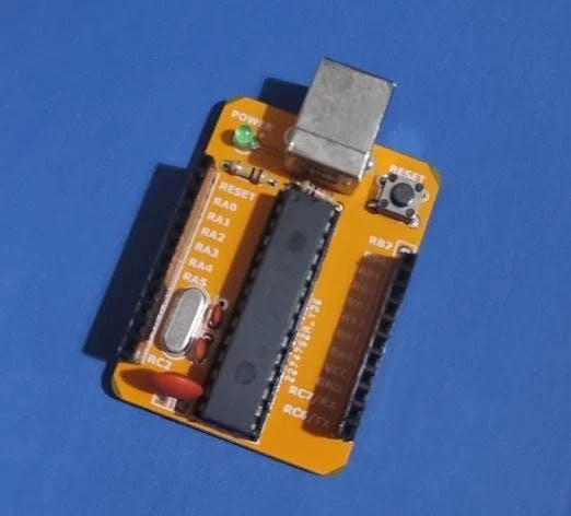
The board module, with the Bootloader firmware, can work in two modes of operation: “Bootloader” mode in which it is ready to be programmed, and “User” mode in which the application program is automatically executed. Both modes are availableautomaticallyonceweconnectedtheboard.
Step 1: MAIN FEATURES
- USB support is the most important feature of self PIC 18f2550; you can have a quick communication with your computer via USB
- Power Led: indicates whether the + 5v USB Supply
- Push button integrated for resetVery affordable to find the componets
- Programming by a small aplication from our PCB
- Interfacing via USB HID (Human interface devide)
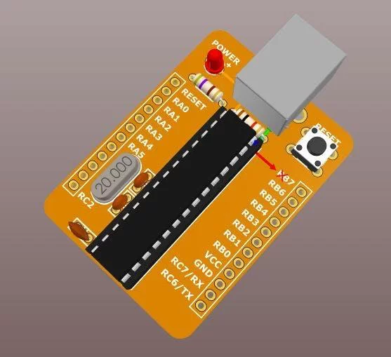
Step 2: SCHEMATIC DIAGRAM
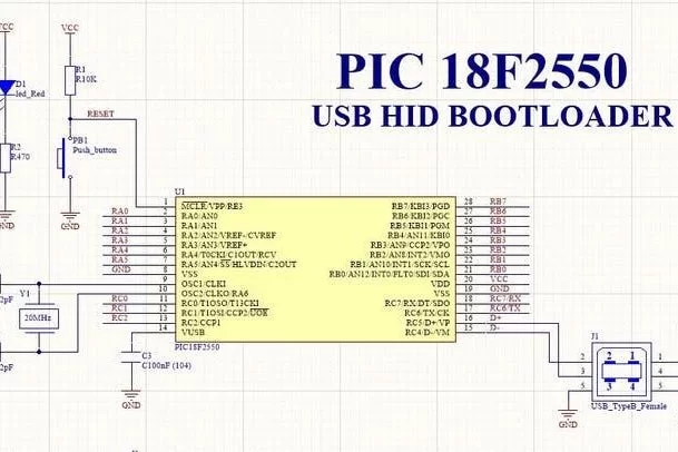
Let’s start with the first step which is the circuit diagram, We should consider this schematic circuit as the base, with the minimal required components, so We are free to add other devices to complete our board according our project’s needs.
►The first part of the schematic is the Pic18F2550, which has the Usb interface, that We are doing to use. As you can see most of the pin has tags or names, it will help to identlfy the important pats or errores.
►Also as We well know, when we work with microcontrolers We need to connect the corresponding oscilator circuit (which consist on 2 capacitors 22pF, 1 oscicaltor 20 MHz)
►The other part of the circuit are the capacitor for the USB interface in this oportunity 220nF (the capacitor should be market with the number )
►We have to add now the pin header in our PCB, these header will let us to connect the microcontroller pins with external devices.
►Finally We should consider a tactile button for reseting the board, and also a led indicator in this case the led indicate that the USB conector is suppling +5v.
Step 3: PCB LAYOUT
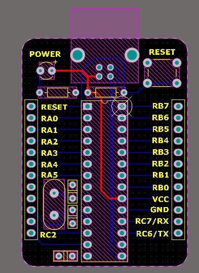
Before We continue with the PCB layout, it is important to indicate that You can use any software for PCB Desing, believe me there are many options, even if you use the best software it will not mean that you are the best pcb desinger, so in this case We are going to use The Altium Designer highly recommended if you want to enter in the pcb design world like a professional.
So after We finished and check our schematic circuit We need to switch from schematic to PCB layout. We can see the PCB with the Ground Plane, this helps for noise filter on the pcb. Also is important to remember that in the case of the microcontroller is necesary to place the crystal and the capacitor the closest possible.
Here after we finish the pcb layout We can get the Gerber files, there are two kind of gerber files we have to pay attention to it, the first GerberX2 and the other Gerber RS274X, most of the manufacturer use the second one Gerber RS274X, in some software we will just GerberX2 and Gerber (In the case of Altium Designer).
You can also download the GerberFiles: Here
Step 4: 3D MODEL
One of the features of Altium Designer is the 3D visualization, the 3d visualization is important and it give us the posibility to see and check our PCB and how it would be in real, also it can show us the components distribution and dimensions. Before I did not consider this feature so important, but the 3d visualization can show us if our footprint dimensions are ok, if all the components will be places without touching each other by mistake.
► Also very important to remember, if you are going to add 3d models, be carefull that you add in the Step AP214 format, the others extensions and formats can not work correctly.
Step 5: PCB MANUFACTURE

Once we finished our development board; it is time to bring it to life. In order to manufacture our board, We are going to use JLCPB Services.In case that you do not have an account yet, check out the bellow link
►JLCPCB: https://jlcpcb.com/IAT
Step 6: ORDER YOUR PCBs ON JLCPCB
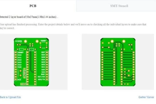
Once We are register, and We logged in our account, We are ready to submit an order and receive our board in a very short time. In this case We need to update first the gerber files, which contains all the necesary information to build the pcb, You can get the gerber files in the link bellow.
►GerberFiles: Here
1. Upload your gerber files
2. Indicate the features
After the upload of our gerber files, We need to indicate the features of the board, in the next picture you can see the options available.
3. Add your shipping address
This part is very important, here you should write your currently address, where you would like to receive your pcb prototypes. It is not common but sometimes very rarely, you will need to pay extra feeds, but as I told you, it is very rarely.
4. Make the payment and finish the order
After you indicates this information, We continue with the payment section, These is the section where you can apply your coupons or discount codes. Basically We can complete the paymente by two general ways, Paypal or Credit card.
5. Receive your PCB
Days later, 7 days or few more, according to your location and custom broker process, You will receive your pcb prototypes.
Step 7: Why JCLPCB?

JLCPCB has been at the fore front of the PCB industry. With over 14-year continuous innovation and improvement based on customers’ need, we have been growing fast, and becoming a leading global PCB manufacturer, who provides the rapid production of high-reliability and cost-effective PCBs and creates the best customer experience in the industry.In case that you do not have an account yet, check out the bellow link►JLCPCB: https://jlcpcb.com/IAT
Most Efficient, Economic, Innovative PCB SolutionsHigher QualityLower CostFaster DeliveryJLCPCB provides a rapid production of high-reliability and cost-effective PCBs and create the best customer experience in the indrustry.
Step 8: THE BOOTLOADER
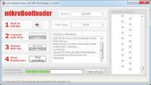
The 18F2550 microcontroller has the possibility to modify its own FLASH memory under the control of a firmware, in a similar way to how the locations in its EEPROM are modified. This firmware is called “Bootloader” and it should be uploaded before to use the board, after uploaded the firmware, We can program directly from our PC to the board. Through this firmware bootloader you will be able to transfer executable programs.hex from the PC to the 18F2550 FLASH memory through the USB cable and using the software application USB HID from Mikroelektronika. This software already has its necessary drivers and automatically detects, through the USB cable, the presence of the board module with the bootloader loaded.
Download the bootloader: Here
Step 9: UPLOADING THE FIRMWARE WITH PICKIT 2
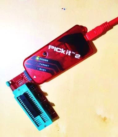
For the first and only time, We are going to use the Pickit 2 Programmer to upload the firmware of our bootloader, once we loaded the.hex firmware, We do not need the pickit 2 again. You can use the Pickit 2, Pickit 3, Pickit 3.5, Pickit 4 or another programmer board available.
Step 10: PROGRAMMING THE BOARD
Now we are ready to program and work with our board, in the below videos You can see how to use our board, basically after We connect, We have 5 seconds to link the board with the bootloader aplications, if we pass the 5 seconds we need to press reset button or connect again the USB cable.
Source: BOOTLOADER WITH PIC18F2550
- How does the board operate?
The board works in two modes: Bootloader mode for programming and User mode where the application program executes automatically upon connection. - What is the most important feature of this board?
USB support is the most important feature, allowing quick communication with a computer via USB HID. - Which software is recommended for PCB design?
Altium Designer is highly recommended for entering the PCB design world as a professional. - Which Gerber file format do manufacturers mostly use?
Most manufacturers use the Gerber RS274X format. - What file format should be used for adding 3D models?
You must add 3D models in the Step AP214 format for correct functionality. - How can I pay for my PCB order on JLCPCB?
Payment can be completed via Paypal or Credit card. - Can I program the board without a programmer after the first time?
No, the Pickit 2 programmer is only needed once to upload the bootloader firmware; subsequent programming is done via USB. - What happens if I miss the 5-second window to link the board?
If you pass the 5 seconds, you need to press the reset button or disconnect and reconnect the USB cable.