Summary of AOI IN PCB & PCBA MANUFACTURING PROCESS OF PCBGOGO
The article discusses the PCB assembly process, emphasizing the challenges with SMT components and the necessity of thorough inspection to reduce defects. PCBGOGO specializes in surface-mount, thru-hole, and mixed-technology PCB assembly, offering quick-turn prototypes and medium to small volume fabrication. Their assembly process includes multiple inspections, IC programming, and software-based functional testing to ensure quality. Automated Optical Inspection (AOI) is a key step used to detect manufacturing defects before shipping. PCBGOGO guarantees that all PCB products comply with industry standards and pass rigorous testing.
Parts used in the PCB Assembly Process at PCBGOGO:
- Through-hole components
- Surface-mount technology (SMT) components
- Conductive pads with solder paste
- Integrated Circuits (ICs) for mounting
- Printed Circuit Boards (PCBs)
- IC programming computer interface
- Automated Optical Inspection (AOI) equipment
PCB assembly consists of many steps. For PCBs with through-hole components, the assembly is quite easy. But for SMT components, elements are placed on the conductive pads with previously applied solder paste that holds the SMT parts together. Then the components are soldered to the pads. Due to the ever-growing demand for high-density circuit boards and smaller SMT components, defects during the PCB fabrication process increase. Thus, a thorough inspection is necessary at many stages of the fabrication process. PCBGOGO is a leading specialist in surface-mount, thru-hole, and mixed technology PCB assembly and electronic manufacturing services, as well as turn-key electronic PCB assembly. PCBGOGO is highly specialized not only in quick-turn PCB prototype and PCB assembly, but also medium and small volume PCB fabrication.

The assembly process at PCBGOGO consists of various inspection and functional verification stages to ensure that the requirements are completely satisfied. During the initial PCB manufacturing process, all the components are inspected by their IQC Department. Before chips are mounted on the PCB, IC programming service is also present. It is usually done by using a computer as a bridge for IC programming. After assembly, functional testing is done by software to ensures that the requirements are satisfied by the application. At PCBGOGO, all PCBs are tested for quality and correctness before shipping.
PCBGOGO team says,
We guarantee that all our PCB products meet industry standards and undergo rigorous testing before delivery.
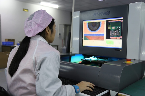
During PCB fabrication, AOI (Automated Optical Inspection) is a crucial process. It ensures that the PCBs leaving the production line are without any manufacturing defects. This inspection is used in PCB fabrication and PCB assembly, as well as testing printed circuit boards.
Read more: AOI IN PCB & PCBA MANUFACTURING PROCESS OF PCBGOGO
