Summary of How to interface LEDs with PIC Microcontroller (PIC18F4550)
This article explains how to interface LEDs with a PIC18F4550 microcontroller by configuring its I/O ports. It details the five ports (A-E), their respective registers (TRISx, PORTx, LATx), and the logic for setting pins as input or output. The project demonstrates blinking LEDs in an alternate fashion using PortB and provides the necessary C source code and configuration steps.
Parts used in the LED Blinking Project:
- LED
- PIC18F4550
It is necessary to understand basic I/O operations of PIC18F4550 before dealing with its complexities. This article presents a way to take simple output from a PIC microcontroller. This learning would also help in interfacing of external devices with the controller. Here the output from the microcontroller is taken on a set of LEDs which are made to blink in an alternate fashion.
PIC18F4550 has a total of 35 I/O (input-output) pins which are distributed among 5 Ports. The following table shows the names and numbers of I/O pins of these 5 ports:
|
Port Name
|
Number of Pins
|
Pins
|
|
PORTA
|
7
|
RA0-RA6
|
|
PORTB
|
8
|
RB0-RB7
|
|
PORTC
|
7
|
RC0-RC2, RC4-RC7
|
|
PORTD
|
8
|
RD0-RD7
|
|
PORTE
|
4
|
RE0-RE3
|
|
|
Bit 7
|
Bit 6
|
Bit 5
|
Bit 4
|
Bit 3
|
Bit 2
|
Bit 1
|
Bit 0
|
|
TRISA
|
–
|
TRISA6
|
TRISA5
|
TRISA4
|
TRISA3
|
TRISA2
|
TRISA1
|
TRISA0
|
|
PORTA
|
–
|
RA6
|
RA5
|
RA4
|
RA3
|
RA2
|
RA1
|
RA0
|
|
LATA
|
–
|
LATA6
|
LATA5
|
LATA4
|
LATA3
|
LATA2
|
LATA1
|
LATA0
|
|
|
Bit 7
|
Bit 6
|
Bit 5
|
Bit 4
|
Bit 3
|
Bit 2
|
Bit 1
|
Bit 0
|
|
TRISB
|
TRISB7
|
TRISB6
|
TRISB5
|
TRISB4
|
TRISB3
|
TRISB2
|
TRISB1
|
TRISB0
|
|
PORTB
|
RB7
|
RB6
|
RB5
|
RB4
|
RB3
|
RB2
|
RB1
|
RB0
|
|
LATB
|
LATB7
|
LATB6
|
LATB5
|
LATB4
|
LATB3
|
LATB2
|
LATB1
|
LATB0
|
|
|
Bit 7
|
Bit 6
|
Bit 5
|
Bit 4
|
Bit 3
|
Bit 2
|
Bit 1
|
Bit 0
|
|
TRISC
|
TRISC7
|
TRISC6
|
–
|
–
|
–
|
TRISC2
|
TRISC1
|
TRISC0
|
|
PORTC
|
RC7
|
RC6
|
RC5
|
RC4
|
–
|
RC2
|
RC1
|
RC0
|
|
LATC
|
LATC7
|
LATC6
|
–
|
–
|
–
|
LATC2
|
LATC1
|
LATC0
|
|
|
Bit 7
|
Bit 6
|
Bit 5
|
Bit 4
|
Bit 3
|
Bit 2
|
Bit 1
|
Bit 0
|
|
TRISD
|
TRISD7
|
TRISD6
|
TRISD5
|
TRISD4
|
TRISD3
|
TRISD2
|
TRISD1
|
TRISD0
|
|
PORTD
|
RD7
|
RD6
|
RD5
|
RD4
|
RD3
|
RD2
|
RD1
|
RD0
|
|
LATD
|
LATD7
|
LATD6
|
LATD5
|
LATD4
|
LATD3
|
LATD2
|
LATD1
|
LATD0
|
|
|
Bit 7
|
Bit 6
|
Bit 5
|
Bit 4
|
Bit 3
|
Bit 2
|
Bit 1
|
Bit 0
|
|
TRISE
|
–
|
–
|
–
|
–
|
–
|
TRISE2
|
TRISE1
|
TRISE0
|
|
PORTE
|
RPDU
|
–
|
–
|
–
|
RE3
|
RE2
|
RE1
|
RE0
|
|
LATE
|
–
|
–
|
–
|
–
|
–
|
LATE2
|
LATE1
|
LATE0
|
|
TRISB
|
TRISB7
|
TRISB6
|
TRISB5
|
TRISB4
|
TRISB3
|
TRISB2
|
TRISB1
|
TRISB0
|
|
Value
|
0
|
…
|
…
|
…
|
…
|
…
|
…
|
1
|
|
TRISB
|
TRISB7
|
TRISB6
|
TRISB5
|
TRISB4
|
TRISB3
|
TRISB2
|
TRISB1
|
TRISB0
|
|
Value
|
0
|
0
|
0
|
0
|
0
|
0
|
0
|
1
|
Project Source Code
###
/******************Chip config*******************
PLLDIV = 5
CPUDIV = OSC1 / 2
USBDIV = 2
FOSC = HIGH_SPEED HS
FCMEN = OFF
IESO = OFF
PWRT = OFF
BOR = OFF
BORV = 3
VREGEN = OFF
WDT = OFF
WDTPS = 1:32768
CCP2MX = ON
PBADEN = OFF
LPT1OSC = OFF
MCLRE = OFF
STVREN = ON
LVP = OFF
ICPRT = OFF
XINST = OFF
DEBUG = OFF
CP0 = OFF, CP1 = OFF, CP2 = OFF, CP3 = OFF
CPB = OFF
CPD = OFF
WRT0 = OFF, WRT1 = OFF, WRT2 = OFF, WRT3 = OFF
WRTC = OFF
WRTB = OFF
WRTD = OFF
EBTR0 = OFF, EBTR1 = OFF, EBTR2 = OFF, EBTR3 = OFF
EBTRB = OFF
******************Chip config*******************/
#include <p18cxxx.h>
void delay_ms ( int delay );
void delay_ms ( int delay )
{
int ms, i;
for ( ms = 0; ms < delay; ms ++ )
for ( i = 0; i < 5; i ++ );
}
void main()
{
TRISB = 0x00; // Set PORTB as output PORT
LATB = 0xFF; // Set PORTB high initially (All LEDs on)
while ( 1 )
{
LATB = ~LATB; // Toggle the value of PORTB
delay_ms ( 1000 ); // Delay of 1 sec
}
}
###
Circuit Diagrams
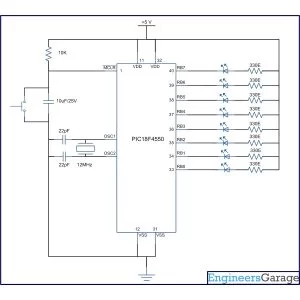
Project Components
Project Video
Source: How to interface LEDs with PIC Microcontroller (PIC18F4550)
- How many I/O pins does the PIC18F4550 have?
The PIC18F4550 has a total of 35 I/O pins distributed among 5 Ports. - What are the three 8-bit registers used to configure each Port?
The three registers are TRISx, PORTx, and LATx. - Which register sets the direction of a port pin as input or output?
The TRISx register is the data direction register that sets the direction of each port pin. - What value sets a pin as an input in the TRISx register?
A High value (1) sets a pin as an input pin. - Where is the data stored that has to be sent to external hardware as output?
The data which has to be sent to external hardware as output is stored in the LATx register. - Can all pins in PortC be used as output pins?
No, Pins 4 and 5 in PortC can only be used as input pins. - What is the function of the RDPU bit mentioned in the text?
The RDPU bit is used to enable or disable internal pull-ups of PortD. - How do you turn off all LEDs connected to PortB in the example code?
You set all the bits of the LATB register Low (0) to turn off the LEDs.