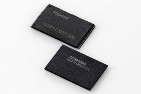
Toshiba is sampling 3D NAND or V-NAND with 48 layers and a 2bit-per-cell architecture delivering a 128Gbit chip.
Toshiba will start volume production of the chip at Fab2 at Yokkaichi which is currently under construction. V-NAND requires a unique tool-set. .
The 48-layer device is aimed primarily at SSD. The more layers you can stack on a V-NAND die, the more cost-effective the technology is. The only people making 3D NAND are Samsung, and they can only make a 128TLC device on a 32-layer stack, which is the same density as it’s getting on its best part on a planar process (19nm) at no better cost.
Obviously no one at Samsung is saying, but V-NAND yields are rumoured to be ruinously poor.
Intel plans to ship a 32 layer 256Gbit MLC 3D NAND in the second half of this year.
Micron, Intel’s technology development partner in V-NAND, is being more cautious than Intel because, it is also rumoured, it can’t get a 32-layer part to yield.
Nonetheless Micron has plans to build a $4 billion 3D NAND fab in Singapore in 2016 and facilitise it in 2017 for shipment in 2017/8.
As the tool-set is unique for V-NAND, the fab will be inappropriate for other product. So, if the yield problems persist, this investment will be wasted.
The problem for planar NAND is that NAND cells have been running out of electrons as they scale down the micron trail. With a few tens of electrons per cell at sub-20nm, NAND behaviour can become unpredictable. Vertical NAND takes that number back up to hundreds of electrons per cell.
For more detail: 48-layer V-NAND from Toshiba
