The ST6G3244ME is a dual supply, low voltage 6-bit bi-directional CMOS level translator for SD, mini SD and micro SD Cards. Designed for use as an interface between baseband and memory cards, it achieves high speed operation while maintaining CMOS low-power dissipation.
The A-port is designed to track VCCA. The internal LDO is powered by VBATand provides a power supply of either 1.8 V or 2.9 V to the B-side I/Os (programmed by the SEL pin). The B-port is designed to track VCCB. The VCCBvoltage can be also used externally. When VCCB= 0 V, there is no additional leakage seen on VCCA. All outputs are push-pull type.
This device is intended for two-way asynchronous communication between data buses. The direction of data transmission is determined by CMD.dir, DAT0.dir and DAT123.dir inputs.
All inputs are equipped with protection circuits against electrostatic discharge, giving them ±2 kV (on A-side) and ±15 kV (on B-side, CD and WP) ESD and transient excess voltage immunity.
Key Features
- Supports 60 MHz clock rate
- Supports DDR mode for SD Card™
- Compliant withSD Specification Part 1 Physical Layer Specification 3.00 (SDR12, SDR25, DDR50)SD Specification Part 1 Physical Layer Specification 2.00
- Bi-directional with direction control pin
- Balanced propagation delays: tPLH≈ tPHL
- LDO power-down support. When the LDO is powered down, VCCBis pulled to GND via the 130 Ω resistor. When VCCB= 0 V, there is no additional leakage seen on VCCA.
- EMI filtering and signal conditioning
- Supports both 1.8 V and 2.9 V data translation on card side
- Integrated LDO to supply 1.8 V or 2.9 V power for B-side I/Os (pin-selectable); can be used also externally
- Integrated pull-up and pull-down resistors on B-side
- Operating voltage rangeVCCA= 1.62 V to 1.98 VVBAT= 3.0 V to 5.0 V
- Latch-up performance exceeds 100 mA (JEDEC Standard 78)
- ESD protection for card side (B-port, CD and WP pins)±8 kV contact discharge (IEC61000-4-2)±15 kV air-gap discharge (IEC61000-4-2)
- ESD protection for host side (A-side)±2 kV HBM (JEDEC 22-A114)±200 V MM (JEDEC 22-A115)
- Operating temperature range –40 °C to +85 °C
- Space-saving Flip Chip 25 package (2 x 2 x 0.605 mm, 0.4 mm bump pitch)
- RoHS compliant, lead-free soldering capable
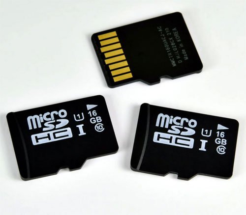
STMicroelectronics claims to have the first voltage-level translator compliant with the latest SD (Secure Digital) 3.0 standard.
The SD 3.0 standard is used for interfacing application processors or digital basebands to SD memory cards in mobile phones, tablets and digital cameras.
The SD 3.0 specification significantly increases storage capacity and access speed. It provides up to 2 terabytes of storage capacity and accelerates SD interface read/write speeds to 50 megabytes per second, at 50 MHz Double Data Rate.
ST’s chip, the ST6G3244, is designed for low power operation and has a data integrity feature using balanced propagation delays and electromagnetic-interference filters and signal conditioning.
The voltage-level translator incorporates 15kV air-gap electrostatic discharge protection on the card side.
For more read: ST supports high speed memory interface in smartphones