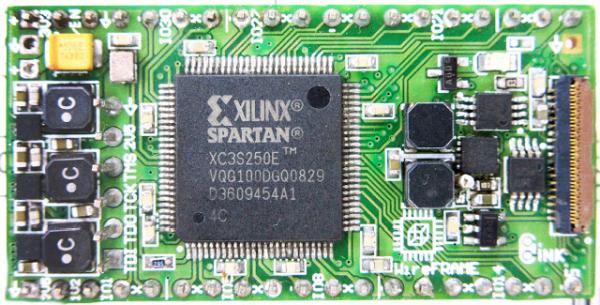
The FPGA Board
The board “WireFrame” has Xilinx XC3S250E at its core ,has 4MByte serial flash for bit-stream storage,32 MByte of SDRam and a small 25Mhz crystal oscillator (can be used FPGA’s DCMs to multiply the clock upto hundreds of Mhz), total 3 2A each power regulator with maximum 6V input ,one regulator each For VccI/O 3.3V , VccAUX 2.5V and VccINT 1.2V. board completely breadboard-able , has two 19pin 0.1” pitch header to be inserted into breadboard. out of total 19 pins there are power input , all 3 regulator’s output, FPGA reset and FPGA I/O them self , few I/O are marked with capability of being configurable as differential pair.a six pin 2.5V JTAG header is separate for FPGA bit-stream download. board comes in very small size of only 50x25mm.
PCB has 4 layers 2 for signal and 2 for power. PCB is designed with trial version of altium and source code gerber file are available for download form github repo https://github.com/circuitvalley/WireFrame-FPGAThe FPGA
the Xilinx XC3S250E it has 250K logic blocks 73Kbit Distributed RAM bits , 360K block ram , 20 Dedicated Multipliers , 4 DCMs. we have used VQG100 package which is very small for such a big FPGA for the shake of small board size. With VQG100 package we got only total 66 I/O (including input only) lines , 30 differential lines. more details how the FPGA is configured to boot ,powered and connected to other peripheral please refer to the schematic.
The DRAM
we have used winbond w9825g6 4 M x 4 BANKS x 16 BITS SDRAM.The RAM is mounted on the bottom side of the board ,it is in TSOP II 54-pin, 400 mil Package
The Serial Flash we have used MX25L3206E , 32Mega Bit , 4 Mega Byte of serial , flash to store bit stream file. it possible to use the Flash to store user Data, but it require some special care need to be taken , as ChipEnable pin of Flash is connected to done pin of the FPGA so after configuration
For more detail: WireFrame FPGA Board , Breadboardable Xilinx XC3S250E Board