
Summary of Voltage Measurement with A PIC Microcontroller
Voltage Measurement with PIC Microcontroller describes using a PIC18F4520 to perform 10-bit ADC-based voltage measurements, covering hardware setup (5V supply, RJ11 serial wiring, 40 MHz crystal, MCLR pull-up) and firmware basics (RA0/AN0 sampling, VDD as Vref, conversion math, and example code). It outlines system integration from power and clocking to ADC conversions and notes omissions like detailed ADC register configuration and signal-conditioning considerations.
Parts used in the Voltage Measurement with PIC Microcontroller:
- PIC18F4520 microcontroller
- 5V regulated DC power supply
- RJ11 jack and wiring for serial communication
- 40 MHz crystal oscillator
- 10 kΩ pull-up resistor for MCLR
- Decoupling capacitors (recommended)
- Series resistors for I/O lines (recommended)
- Analog voltage source connected to RA0/AN0
Voltage Measurement with PIC Microcontroller articulates a methodical framework for facilitating analog voltage measurement using the PIC18F4520, an advanced member of Microchip’s 8-bit microcontroller family. Emphasis is placed on the orchestration of hardware and firmware elements to enable robust analog-to-digital conversion (ADC). The document presents a streamlined system integration process—encompassing power delivery, peripheral interfacing, and digital signal acquisition. Though it presumes baseline proficiency in microcontroller programming and interfacing, it serves as a concise yet effective primer on constructing a minimal analog sensing node, suitable for a broad range of embedded instrumentation applications.
Background:
The PIC18F4520 microcontroller, part of Microchip’s high-performance product line, features a rich peripheral set that includes a 10-bit analog-to-digital converter, enabling the translation of analog signals into discrete digital equivalents. This section introduces its utility within the context of signal measurement, framing the ADC functionality as both integral and easily accessible through minimal circuitry.
By highlighting the operational simplicity and low component overhead of the PIC18F4520, the note implicitly promotes its utility in embedded systems requiring real-time data acquisition. It assumes familiarity with microcontroller programming environments and device flashing protocols but omits granular detail on memory management, compiler toolchains, or pin multiplexing. The overarching goal—enabling the user to digitize external voltage inputs—is positioned not merely as a technical exercise but as a fundamental capability underlying broader signal processing or control applications.
The document’s stated aim of instructing users on RJ11 communication wiring, oscillator integration, and voltage sourcing reflects a comprehensive approach to embedded hardware initialization. Moreover, its practical orientation, culminating in code-based voltage quantification, provides a structured entry point into microcontroller-driven analog measurement.
Connecting the PIC:
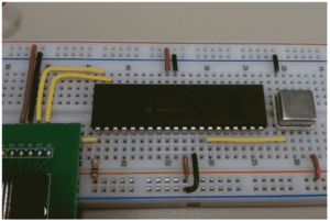
This section delineates the hardware configuration steps essential for initializing the PIC18F4520. The microcontroller is powered via a regulated 5V DC supply, and serial communication is established through an RJ11 interface, which, though unconventional in microcontroller systems, demonstrates a custom implementation of asynchronous communication.

The wiring instructions are pragmatic and deliberate. Pin mappings from the RJ11 to the microcontroller ensure bidirectional data exchange capability, while the connection of VDD and ground to both the microcontroller’s core pins (11 and 32 for VDD; 12 and 31 for VSS) guarantees electrical symmetry and noise rejection. The use of a 40 MHz crystal oscillator—in lieu of an internal oscillator—enables precise clock generation, an essential requirement for time-sensitive tasks like ADC sampling. The document correctly orients the oscillator based on its notched packaging and assigns proper grounding and VDD routes for stable oscillation.
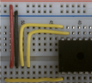
Furthermore, the incorporation of a 10kΩ pull-up resistor on the MCLR (Master Clear Reset) line is a canonical design element, ensuring that the microcontroller remains operational by avoiding unintended reset states. This segment successfully captures the essence of minimal viable hardware configuration necessary to support stable execution and peripheral interfacing.

The wiring schema, while functionally adequate, would benefit from schematic illustrations or pin-out diagrams to augment textual descriptions. Additionally, considerations such as decoupling capacitors for noise suppression or series resistors for signal integrity on I/O lines could be introduced to reflect industry-standard best practices.
Writing the Code:
This section introduces the firmware logic required to facilitate analog voltage acquisition through the ADC subsystem. The analog voltage is sampled from pin 2 (RA0/AN0), and VDD is used as the positive reference voltage. This configuration results in a 10-bit digital output, quantized across the range , directly proportional to the analog input with respect to the supply voltage.
The mathematical expression:
Analog Voltage=(Digital Value1024)×VDD\text{Analog Voltage} = \left( \frac{\text{Digital Value}}{1024} \right) \times V_{DD}
is derived from the linear transfer characteristic of the SAR (Successive Approximation Register) ADC architecture. An example calculation yielding 4.32V from a digital value of 884 demonstrates the precision achievable under ideal operating conditions.
However, the discussion abstracts away the microcontroller’s register-level control of the ADC module. Critical details such as configuration of ADCON0 for channel selection and ADC enablement, ADCON1 for reference voltage configuration and port direction settings, and ADCON2 for acquisition timing and conversion clock settings are omitted. These registers are central to ADC functionality and should be explicitly documented to ensure deterministic and error-free operation.
Moreover, sampling considerations—such as impedance of the voltage source, required acquisition time (TACQ), and sample-and-hold capacitor stabilization—are absent, yet play a significant role in real-world analog measurement fidelity. Without this, the risk of aliasing or conversion artifacts increases, especially in applications with dynamic or noisy signals.
The final code logic, although not fully provided, presumably employs a polling-based acquisition scheme. A more advanced implementation might consider interrupt-driven conversion, DMA-based transfers, or oversampling techniques for increased resolution.
#include
include  #
#include
#pragma config LVP=OFF
#pragma config WDT=OFF
void rx_handler (void); //Declare the ISR function
int adc_result; //The variable to store the ADC value in
void main()
{
RCONbits.IPEN = 1; /* Enable interrupt priority */
IPR1bits.RCIP = 1; /* Make receive interrupt high priority
INTCONbits.GIEH = 1; /* Enable all high priority interrupts
OpenADC(ADC_FOSC_32 & ADC_RIGHT_JUST & ADC_12_TAD,
ADC_CHO & ADC_INT_OFF, 0); //open adc port for reading
ADCON1 =0x00; //set VREF+ to VDD and VREF to GND (VSS)
while(1)
{
ConvertADC(); //perform ADC conversion
while (BusyADC()); //wait for result
adc_result = ReadADC(); //get ADC result
// adc_result is the digital representation of the voltage at pin2
// it is a number out of 1024 that specifies a fraction of VDD
///
}
}
Conclusion:
The conclusion succinctly encapsulates the core contributions of the application note—namely, the successful configuration of the PIC18F4520 microcontroller for rudimentary analog voltage acquisition, and the demonstration of code logic for converting raw ADC output into a meaningful analog representation. It highlights the end-to-end implementation pathway, from hardware initialization (wiring, clocking, and power distribution) to firmware execution (data conversion and scaling), thereby presenting a minimal yet functional embedded sensing system.
While the scope of the implementation remains foundational, the concluding remarks wisely underscore the extensibility of the technique. The ADC subsystem, once initialized and operational, serves as a reusable interface for numerous embedded contexts. By integrating this analog acquisition methodology with additional logic structures—such as threshold detection, feedback control, or digital communication protocols—developers can construct more sophisticated, event-driven or closed-loop systems.
However, the conclusion stops short of acknowledging limitations or opportunities for refinement. For instance, it could briefly mention potential sources of inaccuracy (e.g., reference voltage drift, input impedance mismatch, ADC noise floor) or propose enhancements (e.g., implementing calibration routines, using differential inputs, or incorporating signal filtering).
Quick Solutions to Questions related to Voltage Measurement with PIC Microcontroller:
- What microcontroller is used for the voltage measurement project?
The project uses the PIC18F4520 microcontroller. - How is the microcontroller powered?
The microcontroller is powered from a regulated 5V DC supply connected to VDD and VSS pins. - Which pin is used for analog input?
Analog input is sampled from pin 2, RA0/AN0. - What reference voltage is used for ADC conversions?
VDD is used as the positive reference voltage and VSS (ground) as the negative reference. - What clock source is recommended?
A 40 MHz crystal oscillator is used in the design for precise clock generation. - Why is a 10k pull-up resistor used on MCLR?
To keep MCLR high and prevent unintended resets, ensuring the microcontroller remains operational. - How is the ADC value converted to analog voltage?
Analog Voltage = (Digital Value / 1024) × VDD, using the 10-bit ADC result. - Does the article include full register-level ADC configuration?
No, it notes that detailed ADCON0, ADCON1, and ADCON2 register configurations are omitted. - What additional hardware practices does the article suggest but not detail?
It suggests using decoupling capacitors and series resistors for noise suppression and signal integrity, but does not provide specifics.
