Simple expansion board for 8051SBC provides easy USB port and graphic LCD interface.
I am planning to design the x86 board for some of my application that needs more computing capability. One of the features that I need to add to the x86 board is the USB port. I found the ASIC that enables 8-bit MCU to interface USB easily from Future Technology Devices International: FTDI. The USB controller chip is FT245BM. Fortunately, near my campus, the Astron Logic company sells the ready board for such a USB chip with a connector. So I bought it to learn how to interface with 8051SBC. Also, I got one graphic LCD 128x64pixels. I thought why don’t put them together and build the expansion board for testing with 8051SBC. This led me to provide details of what I have done. However, no real application with the 8051SBC has been completed yet. Below was the sample hardware and some testing code only.
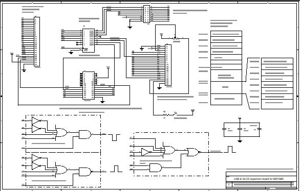
Hardware Schematic
J2 is a 24-pin header, you may see the signals on J2, it provides necessary signals for memory-mapped I/O expansion. Those signals include:
Data bus: D0-D7,
Address bus: A0-A4, A8,A9,A10, and A15,
Control bus: /RD, /WR, RESET, /INT0, /INT1,
Power supply: +5V and GND.
The data bus, D0-D7 signals are tied to both FT245BM and GLCD data bus directly.
Figure 2: Hardware schematic of the expansion board.
The enable signal for USB chip and GLCD controller were made by PLD decoder from the address lines. As we have seen the memory map for i/o of 8051SBC board, the available space is from 0x0300-0x07FF. The address range of 0x0300-0x03FF was used for USB chip for both RD and WRITE operations. The GLCD used 0x0400-0x04FF with A0-A3 for selecting the internal registers from 0x0404-0x040B.
We have learned from 8051SBC on how to use PLD as the memory decoder. In the schematic you may see the equivalent logic symbol for each enable signal. Let study the logic equation shown in Figure 3 and the equivalent logic circuit, you will understand how easy it is.
| ; USB8051SBC PLD Equation ; Memory and I/O decoder for USB&GLCD expansion Board ; Wichit Sirichote, [email protected] ; Dec 13, 2003 ; PLD: Lattice GAL16V8DCHIP 8051SBC GAL16V8 a15=1 rd=2 wr=3 a8=4 a9=5 a10=6 glcd_enable=17 rd_usb=18 wr_usb=19 RST=7 LCD_RST=16 EQUATIONS /glcd_enable = rd * wr + a8 + a9 + /a10 + a15 /wr_usb = /a8 + /a9 + a10 + a15 + wr rd_usb = /a8 + /a9 + a10 + a15 + rd LCD_RST = /RST |
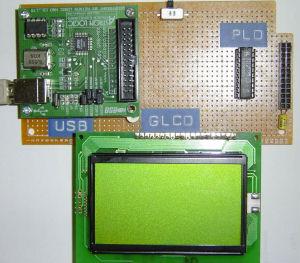
 Board Layout
Figure 4 shows the sample layout made by universal pcb. We see that with a PLD, the glue logic will be put together in PLD chip. The left-hand, J4 is 26-pin connector for USB board. And the bottom connector, J3 is 20-pin SIP connector for GLCD board. The right-hand connector J2 is for 8051SBC expansion header. Upper is manual switch for backlight turn on/off.
Ezy USB-M01 Board
Figure 3 shows the USB module made by Astron Logic Company. The evaluation kit consists of USB board, user manual, cable and software CD for driver and test software. The kit is available at low-cost, to get it please contact Astron Logic directly.
The USB board is based on FT245BM. The chip provides complete hardwire USB protocol that conforms USB1.1 and USB 2.0 (full speed mode). The FT245BM can learn more from Future Technology Devices International: FTDI.
For more detail: USB & GLCD expansion board for 8051SBC