Summary of The IDE Project
The author repaired a crossed-line prototype board to create a semi-portable IDE project using a PIC microcontroller and Compact Flash adapter. The system features high-speed data transfer via low-level assembly routines, currently reaching 430kb/s, with a VT100 serial terminal interface planned for future I2C integration.
Parts used in the IDE Project:
- Prototype boards
- Solder and wire
- PC power supply (AC outlet)
- Compact flash adaptor
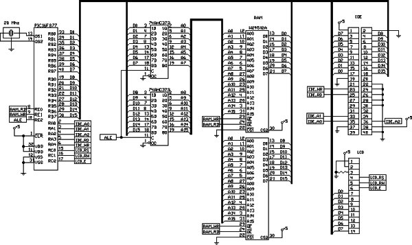
- PIC microcontroller
- IDE header
- 74LS373 chips (2 units)
- 64kx8bit cache ram chips (2 units from old 486 motherboard)
- LCD display
- 8MB CF card
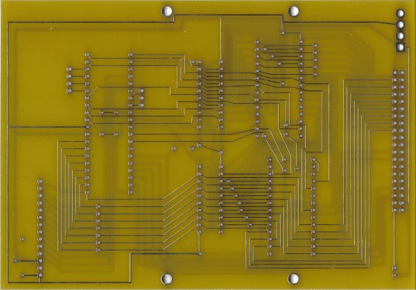
4 prototype boards arrived today. After going over them carefully, I found 4 lines that crossed each other. After some quick surgery with a knife and some solder and wire, the IDE project is now semi portable. The power supply is still out of a PC, so it’s tied to an AC outlet. I’d like to make it battery powered or at least get a smaller power source on it so it’s more easily moved.
There’s mounting holes for standoffs so it can piggyback with a hard drive. Right now, I’ve got the compact flash adaptor mounted on it.
I’ve been spending every waking moment for the last 3 weeks working on this project. The low level assembly routines have been done for a while. I’ve just been delaying putting them here. My main focus right now is finishing this project in Optama C. I’m working on something I’m going to call PICDOS. So far, I have about 14 commands defined and am working on writing the code behind those commands. For testing purposes, the user interface is a VT100 serial terminal using the built-in USART. Eventually that interface will be replaced with an I2C interface so a microcontroller (such as the BS2) can easily access a FAT partition with minimal hassle.
Here’s the low-level routines wrapped in a C function call:
low.c
-
How can the IDE project be made more portable?
The author wants to replace the current PC power supply tied to an AC outlet with a battery or smaller power source. -
What is the current data transfer speed achieved by the assembly code?
The assembly code allows for transfers of 430kb/s from the drive to RAM. -
How long does it take to read an entire 8MB CF card?
The system can read the entire 8MB CF card in less than 19 seconds. -
What interface is currently used for the user interface?
The user interface is a VT100 serial terminal using the built-in USART. -
What interface will eventually replace the current user interface?
The interface will eventually be replaced with an I2C interface to allow easy FAT partition access. -
Why were NOPs inserted into the code?
NOPs are being considered to resolve timing issues because the PIC is faster than the CF card. -
How much RAM is arranged in the new PIC version?
The setup uses 128kb of RAM arranged to latch the whole 16-bit address and read/write a whole word of data at a time. -
How many pins on the PIC are currently being used?
So far, 24 pins out of the 33 available on the PIC are being used.