Summary of Rubidium Atomic Clock
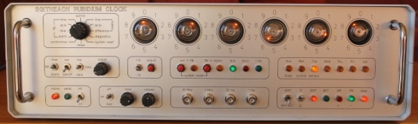
This article details the construction of a vintage-inspired atomic clock featuring Rubidium frequency standards and Dekatron vacuum tube displays. The project evolved from 2008 to 2012, incorporating hardware upgrades like new PCBs and software revisions for robustness. It utilizes a Datum LPRO rubidium oscillator for precision timing, an ATMEGA microcontroller for logic, and Russian OG4 or GC10B dekatrons for the visual display. The design includes extensive front panel controls, a gong chip for chimes, and dual power sources including mains and battery backup.
Parts used in the Rubidium Atomic Clock:
- Datum LPRO Rubidium Oscillator
- PCF8583 Clock Chip (Legacy)
- ATMEGA168 Microcontroller
- GC10B Dekatrons
- Russian OG4 Dekatrons
- 74HC390 Divider Chips
- LT1016 Fast Comparator
- PCF8574 I/O Expanders
- GAL16V8 Logic Gates
- SAE800 Gong Chip
- ATMEGA644P-20 Main Microcontroller
- Toroidal Transformer
- Batteries for Power Backup
Introduction
In the 1970s I worked for a while for the UK Atomic Energy Authority (UKAEA) at a site in Winfrith, Dorset. Amongst a lot of other interesting work, I used a gamma ray density gauge that amounted to a caesium-137 source, in its castle and collimator, the target (various), a sodium iodide detector (from memory), a photomultiplier and a series of counters using dekatrons. Having spent hours taking readings off the dekatron counters I somehow still associate dekatrons with things “atomic”…
Precision frequency generators using the rubidium atomic frequency standard have been around for many years; second hand units have found there way on to Ebay at modest (circa $100 US) prices. I have built a number of clocks of varying accuracy – time set using Internet time standards, time set by GPS and using a humble crystal oscillator. So an alternative would be to use a clock based on a Rubidium atomic frequency standard. This would have the small advantage of being accurate (once set) without requiring external intervention (as the Internet and GPS clocks require).
Having seen other “atomic” nixie clocks (nixiebunny and jthomas as examples) it perhaps came naturally (to me anyway) to use dekatron as the clock display. Dekatrons are not as common as nixies in clocks using glowing neon but examples are around on the net (Bill (about a 3rd down the page), Jason Harper).
Lastly, I wanted a clock with as many switches, buttons and lights as I could manage (as against imagine which could be a nightmare).
Revision history (February 2010 – December 2012)
The first version of this clock I built during 2008 with these webpages first published in February 2009. During the last few year I have tinkered with the clock to resolve a few hardware problems. The main changes have been to
- work with both 50 and 60Hz mains frequencies
- improve the chime sequence repeat rate
- improve the high voltage switching arrangements
- allow Russian OG4 dekatrons as well as orginally GC10B dekatrons to be used
- giving the software a complete workover to make it more robust
- write a series of test programs so individual subsystems could be independantly and fully tested
- replace the front panel with a laser cut/engraved one
- rewrite the software using the free GCC-AVR C Compiler
 These changes have resulted in the divider and main microcontroller boards being first adapted and eventually replaced and a few trivial changes to the interboard wiring. Only the new boards and their software will be described below the legacy cards are all abandoned although the old front panel design is still available (within the Eagle file download).
In reworking this webpage I have also added more information on the construction and front panel wiring.
The divider card software, dekatron card software, test software and final clock software are all now available for download.
Atomic Clock
The rubidium oscillator I bought on Ebay is a Datum LPRO.
A microwave signal is derived from a 20MHz voltage-controlled crystal oscillator (VXCO) and applied to the rubidium (Rb 87) vapour within a glass cell. The light of a rubidium spectral lamp also passes through this cell and illuminates a photo detector. When the frequency of the applied RF signal corresponds to the ground-state hyper-fine transition of the Rb87 atom, light is absorbed, causing a decrease in the photo detector current . The dip in photo detector current is used to generate a control signal with phase and amplitude information which permits continuous atomic regulation of the VXCO frequency. The VXCO signal is divided by 2 and fed through a buffer amplifier to provide the standard frequency output of 10 MHz.
To me it is just a “black box”, feed it correctly and it produces a precision 10MHz sine wave. It does produce some other diagnostic signals to show the unit is healthy:
- BITE Built In Test Equipment signal to show the VCXO is locked to the atomic transition. As long as BITE is low once the unit has warmed up, the output frequency is within roughly ±5E-8 of absolute frequency.
- LAMP V signal monitors the inherent degredation of the lamp light pickup; this signal should be >3 volts and < 14 volts.
- XTAL V MON signal can be used to show if the crystal is drifting out of the available trim range; this signal should be > 0.55 volts and < 12.6 volts.
When I hooked a power supply up to the second hand unit, I was pleased to find the BITE signal when low after a few minutes (lock achieved) and the LAMP and XTAL voltages were both roughly mid range (in my ignorance I assume this is good).
By “feed it correctly” the LPRO requires a 24v peak 1.7A, normal 0.5A; power supply. The clock requires more than a 10MHz oscillator so I originally decided to use the a PCF8583 clock chip. This chip will accept a 50Hz signal (so I need a divide by 200,000 to get 50 Hz from 10 MHz) and communicates with a microcontroller using TWI (I²C) interface. I decided to pinch the nixiebunny idea of using batteries to preserve clock operation during power loss. The batteries would be float charged but capable of running the rubidium oscillator (0.5A at 24V) and the miscellaneous divider chain and clock. Then a thought occurred – why not measure time using mains frequency in a second PCF8583 clock chip so that absolute and long term differences between “mains” and “rubidium” could be measured. This arrangement has one disadvantage – there is no 60Hz mains version of the PCF8583 available and I have received interest from LandOf60Hz in replicating the clock. So I kept the legacy of dividing 10 MHz to 50 Hz (as I explain below I needed to divide to 1 Hz anyway) but swapped the two PCF8583 clock chips with a single ATMEGA168 to count transitions from the divider chain or from filtered mains and to communicate the count using a TWI interface. (On the way I considered using something like a ATTINY13 programmed as a “60Hz” PCF8583 but this seemed an overly complex solution.)
Finally, I wanted front panel outputs of the various frequencies available down to 1 Hz (so the divider chain would be divide by 10,000,000 in total). The first PCB for the clock was now evolved:
- 24 VDC and 5 VDC power supply
- Mains (float charged) battery
- 10 MHz buffer (design from LPRO manual using a LT1016 fast comparator)
- Divide to 1 Hz in a series of divide by 2 divide by 5 steps (74HC390)
- Buffered outputs at 10 MHz, 1 MHz, 50 Hz, 1 Hz
- ATMEGA168 chip linked (interrupt) to rubidium 50 Hz divider output and linked to filtered and squared 50/60 Hz mains frequency
- Sensing BITE (“locked”), LAMPV (“lamp”), XTAL V MON (“crystal”) signals by the ATMEGA168
- TWI link to the main microcontroller (clock counts, sensed values)
- 1 Hz interrupt from the Rb oscillator derived clock
- LEDs to indicate oscillator lock (BITE low), 1 Hz pulses from the two clock sources and an error status
- Off board would be a 18 + 18 VAC 50VA torriodal transformer
Divider Schematic and PCB layout
Right click and then “save as” to see these images at higher resolution. The board Eagle files are available for download below. I built the board up first and tested it with an ATMEGA32 based test card to check the mega168 clock could be addressed and that all of the required signals were available. Everything was OK so I moved on to the dekatron display cards.
In electronics, a Dekatron (or Decatron, or generically three-phase gas counting tube or glow-transfer counting tube or cold cathode tube) is a gas-filled decade counting tube. Dekatrons were used in computers, calculators and other counting-related devices during the 1940s to 1970s. The dekatron was useful for computing, calculating and frequency-dividing purposes because one complete revolution of the neon dot in a dekatron means 10 pulses on the guide electrode(s), and a signal can be derived from one of the ten cathodes in a dekatron to send a pulse, possibly for another counting stage. Sending pulses along the guide electrodes will determine the direction of movement.Internal designs vary by the model and manufacturer, but generally a dekatron has ten cathodes and one or two guide electrodes plus a common anode. The cathodes are arranged in a circle with a guide electrode (or two) between each cathode. When the guide electrode(s) is pulsed properly, the neon gas will activate near the guide pins then “jump” to the next cathode. Pulsing the guide electrodes repeatedly will cause the neon dot to move from cathode to cathode. The dekatron fell out of practical use when transistor-based counters became reliable and affordable. Today, dekatrons are used by electronic hobbyists in simple “spinners” that runs off the mains frequency or as a numeric indicator for homemade clocks.
To operate the dekatrons you need several things:
- High voltage for the anodes (typically 375 – 400 volts above the cathode voltage)
- An intermediate voltage to hold the guide electrodes positive with respect to the cathodes
- A means to take the guide electrodes to a voltage much lower than the cathodes so that the glow is transferred on to it
- A means of detecting that cathode zero is glowing
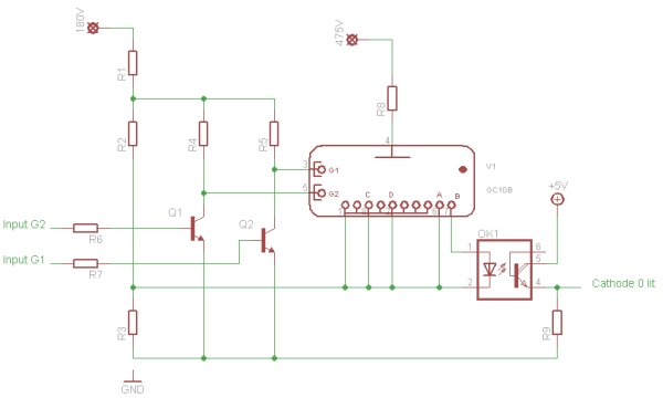
This circuit shows the principles (from an original design by Mike Moorrees):
The cathodes are held a a positive voltage with respect to ground (this will avoid requiring a negative supply). A signal on one of the two inputs will bring the guide electrode down to a voltage negative with respect to the cathodes and so the glow will transfer onto that guide. Sequencing the pulses onto the two inputs will make the glow rotate in either a clockwise or anti clockwise direction. When cathode zero is glowing (B output on a GC10B dekatron) the cathode 0 lit output will go high.To rotate the glow the following sequence is needed:
- Starts with inputs G1 and G2 both low
- Make Input G1 high
- Wait a few 100 μS – dekatrons are relativily slow – glow moves to G1 electrode adjacent to the glowing cathode
- Make Input G2 high
- Wait a few 100 μS – glow becomes “shared” between the two guide electrodes
- Make Input G1 low
- Wait a few 100 μS – glow moves to G2 electrode
- Make Input G2 low – restoring the original state
- Wait a few 100 μS – the glow moves onto the cathode adjacent to the G2 electrode
- Success – the glow has moved from one cathode to another!
By sequencing the guide electrodes in the opposite order (G2 first) the glow will rotate in the opposite direction. Since on start up the cathode that glows first is unknown it is simple to rotate the glow using this sequence until a high is detected on the cathode 0 lit output; the dekatron is now in a known state (zero).So six dekatrons (hours : minutes : seconds) requires 12 outputs and 6 inputs from a micro controller. This is fairly heavy demand of I/O pins if I was using a single ATMEGA644P (as intended) which has 32 I/O pins. Since I was already using an TWI interface for the clock chips it seemed logical to look at using TWI port expanders. The PCF8574 expander has 8 I/O pins so irratingly I would need 3 chips. An alternative was to use, say, an ATMEGA168 as an TWI slave. This chip can be arranged to have upto 23 I/O pins – I need 18 for the dekatrons, 2 for the TWI, 1 for the reset (so I can use my usual programmer) and that makes 22 pins used – with 2 spare. I will use the internal 8 MHz RC oscillator which is good enough for this application. I use the “not for profit” version of Eagle which limits me to 160 x 100mm boards. To space the 6 dekatrons out sufficently I needed to space the design across two PCBs (which I actually cut to 150 x 100mm). An early design arranged the dekatrons in a 3 x 2 pattern rather than the straight 6 used here – I din’t like the resulting front panel designs, although the dekatrons the fitted onto a single 160 x 100 mm board. Links connect the first and second boards together. The ATMEGA168 is on the first board. The software would configure the ATMEGA168 as a TWI slave, would handle all the glow movements and accept commands like “move glow on dekatron 3 to position 2”. This would only take 2 bytes on the TWI bus. Other commands would set all glows to position zero (1 byte), set all 6 dekatrons to given positions (7 bytes) and also to force the ATMEGA168 to reset (1 byte). This all looked simple enough but I made the data structure more complex by adding a simple CRC7 checksum to make the communication more robust. This added a single byte to each command.
One spare input pins is arranged to put the card into a self test mode if grounded (eventually I may to use the second pin for some purpose).
GC10B version
Note the orientation of the octal sockets so that pin 6 is uppermost. This pin corresponds to cathode 0 which will then be at the top.
OG4 version
I have also produced a version of the cards to use the Russian OG4 dekatron which are currently in more plentiful supply than GC10/B dekatrons. The OG4 supply (on EBay, at the time of writing this) is for NIB dekatrons whereas the GC10B available tend to be (well) used – often electrode zero is entirely eroded away.
Note the orientation of the octal sockets so that the spline is uppermost. This pin corresponds to cathode 0 which will then be at the top.
Main Power Supply
I chose to use the same power supply I had used successfully with the bookcase clock that used a dekatron as well as four nixies. This would deliver the required voltages for the remainder of this clock when using a 15VA 18-0-18 VAC torroidal transformer. The power supply is physically large compared with other designs but I have plenty of space in the case I planned to use (more on the case selection and final assembly below).
I wanted to be able to turn off the dekatrons (to extend their life) when the clock was not in use but leave the rest of the clock running. I therefore added a relay to switch the AC feed into the voltage multiplier. I added a neon bulb as a warning indicator when the multiplier held a charge: touching the 475 V supply would smart to say the least… Not much else to say about power supply other than I added an on/off switch and fuse on the mains side of the two transformers together with a small (3A) LC filter to remove any rubbish on the mains. QED.
Main Power Supply Schematic and PCB Layout
Right click and then “save as” to see these images at higher resolution. The board Eagle files are available for download below.
Front Panel IO
The penultimate card is the front panel I/O. This uses four PCF8574 8 bit TWI I/O expanders to give 32 control lines. Since I was planning on a large number of front panel switches and neons I knew I was going to go beyond the I/O capabilities of the micro controller I planned to use. An alternative would be to use a third microcontroller as another TWI slave but I have a tube of PCF8574 chips available and they would provide the required I/O together with an interrupt signal to the main microcontroller when a switch was moved so I would not have to poll all of the switches in the software to detect changes. The main clock mode switch (clock, timer, alarm, sync, spinner etc) was to have 12 positions so I have used a GAL16V8 as a 12 to 4 encoder – there are many ways of achieving this kind of encoder but I have a good supply of these and other GALs (bought cheaply on Ebay). On the output side, I intended to have 7 neons to show the day of week (as well as some diagnostics) but only one of these would be lit at any time, so I used a second GAL16V8 as a 3 to 8 decoder. To generate the JEDEC data for the GALs I use the free Atmel WinCUPL compiler and a second hand programmer (again bought on Ebay). The WinCUPL input and output files are available for download below.
One last tweak was that I wanted all of the front panel switches to have their common pole connected to ground whereas the power supply needs a 5V positive signal to switch the HV relay on. So I used two free pins on the first GAL to form an inverter so grounding its input produces a 5V output (this output is unused after the 2010/11 revision).
 Main Microcontroller
The last board to describe is the main micocontroller board. The board has the following facilities:
- RS232 interface to be able to synchronise the rubidum clock with an external time source such as a GPS unit or NTP Client, to link to a PC for diagnositics and other setup and to provide a serial link to a data network (for example using RS485)
- SAE800 gong chip to generate tones for alarms, hour chimes etc
- A TWI interface for use within the clock to communicate with the front panel controls, the dekatrons and the clock TWI slaves (all described above) (brought out on two headers)
- Interrupt inputs from the rubidium oscillator timed clock to give an accurate 1 interrupt per second and an interrupt from the front panel I/O expanders that will interrupt to signal that front panel switch has been moved
- 4 way DIL switch to options that I would not anticipate changing very often (in that you need to open the case)
- 3 LEDs for simple diagnostics and testing purposed
- A rotary encoder to be able to adjust clock alarm and timer settings
- A hardware reset button
- A whole spare port (Port A) brought out to a box header
- Finally, a programmer socket (in-situ programmer or ISP)
I selected an ATMEGA644P-20 (to be slightly overclocked at 22.1184 MHz) as it contains a genererous amount of flash, SRAM, EEPROM (not that I envisaged using much EEPROM use in this project) and sufficient I/O pins, UARTs etc for all of the facilities listed above. Again, here is the schematic and PCB layout (another double sided board) to view and the designs are in the Eagle download file.
Main Microcontroller Schematic and PCB
Right click and then “save as” to see these images at higher resolution. The board Eagle files are available for download below.
SAE800 Gong Chip
The gong chip is probably worth a special mention as it is a simple way to get single, dual or triple gong tones. In the triple tone mode the notes, for example can be arranged as the minor and major third: e2 – c# – a, corresponding to 660Hz, 550Hz and 440 Hz.
The gong chip allows the tone fundamental frequency and volume to be adjusted by setting two resistor values, so I decided to bring these out as variable resistors on the front panel (well why not?). Here is a (crude) recordings with a microphone of the gong chip in action:
The gong chip is simple to use and triggering it is easy in the software. The downside is that it is a bit municipal rather than musical.
For more detail: Rubidium Atomic Clock
- How does the rubidium oscillator maintain accuracy?
A microwave signal derived from a VXCO is applied to Rb87 vapour; light absorption at the hyper-fine transition generates a control signal to regulate the frequency. - Can this clock operate with both 50Hz and 60Hz mains frequencies?
Yes, the revised design allows work with both 50 and 60Hz mains frequencies by counting transitions from filtered mains. - What is the function of the BITE signal?
The BITE signal indicates if the VCXO is locked to the atomic transition; when low after warm-up, the output is accurate within ±5E-8. - How are the dekatrons rotated to display numbers?
The glow is transferred between cathodes by sequencing pulses onto two guide electrodes (G1 and G2) in a specific timing pattern. - Why was the PCF8583 chip replaced with an ATMEGA168?
The replacement was made because no 60Hz version of the PCF8583 exists, allowing a single chip to count from both divider chains and mains. - What type of transformer is used for the power supply?
An 18 + 18 VAC 50VA toroidal transformer is used to generate the required voltages for the circuit. - How does the system handle time during a power loss?
Batteries float charged by the power supply run the rubidium oscillator and divider chain to preserve operation. - What components allow for extensive front panel switches?
Four PCF8574 8-bit TWI I/O expanders provide 32 control lines to manage the numerous switches and neons. - How is the chime sound generated?
An SAE800 gong chip generates tones for alarms and hour chimes, with volume and frequency adjustable via resistors. - What is the purpose of the GAL16V8 chips on the front panel?
One GAL16V8 acts as a 12-to-4 encoder for the main mode switch, while another serves as a 3-to-8 decoder for day-of-week indicators.