The ATMega168 is a great general purpose 8-bit AVR microcontroller from Atmel. It has 23 GPIO pins, but sometimes (as I have found) you can run out of I/O pins as your design grows. This happened to me recently when, of the 23 GPIO pins available, 2 were taken up by an external ceramic resonator, 1 for the reset line, 3 for serial coms, 14 for the LCD, and 3 for RGB LED control. This used all 23 GPIO pins, with none left for the four buttons I needed. What to do? This Design Idea has the solution.
A close look at the ATMega168 data sheet revealed that the I/O pins available on the 28-pin DIP package and on the 32-pin TQFP package are not all the same. On the TQFP package, there are an additional pair of VCC & GND pins and an additional two ADC input pins on top of the advertised 23 GPIOs. So if I could read my 4 buttons with these extra ADC inputs, all would be OK and the design would be saved.
Now, the user interface was fairly overloaded with functions, and various combination button pushes were used to call up different menus on the LCD. Also, the software was still under development and more combination button pushes might be called for. I wanted to be able to detect each button individually as well as all possible button push combinations, so for four buttons, I needed to detect a total of 24, or 16 possible button states.
OK I thought, that should not be hard. I just need a resistor network between my four buttons and one of the ADC inputs so each button pulls down a different amount and all 16 combinations are evenly spaced between VCC and GND (Figure 1). However when I tried to do this it turned out not to be as easy as it looked at first sight.
I considered using an R2R resistor ladder, but this requires SPDT buttons so the inputs are connected to VCC or GND, not left floating. After thinking about this for a while, I realised I was making things more difficult for myself than I needed to. There are two ADC inputs available, so if I put only two buttons on each input, then each would only need to detect 22, or 4 possible button state combinations instead of 16 (Figure 2). If the states are not evenly distributed between VCC and GND, it would not matter too much.
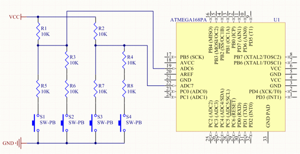
This resulted in the circuit of Figure 3, which proved a successful solution and has now been in production in my client’s product for some time. The resistors are all the same value, so a four-resistor network like this Bourns 1206 part can be used for a small, neat solution.
The spreadsheet in Figure 4 details the operation of each circuit (download the design files at the end of the article). The yellow cells are where you enter the resistor values used, the supply voltage, and the ADC resolution. The green cells are calculated outputs showing the operation of the circuit. The first three columns show a truth table of the button inputs, and the R Buttons column shows the total pull-down resistance resulting from the different button combinations. The Vout and Counts columns show the voltage input to the ADC and the resulting ADC reading. Count Mid Points shows values midway between the expected ADC values – it is these that are used to differentiate the different inputs and decode the button pushes. This ensures that all possible input values are decoded and maximum allowance is made for variation due to resistor tolerance, noise, etc.
The software decodes which combination of the four buttons is pushed, debounces the button inputs, and handles button repeat operations when certain buttons are held down.
As can be seen, the code distribution is not at all linear. However, even the closest values still maintain a reasonable separation for practical operation. A graph of the results (Figure 5) shows the nonlinearity and also highlights that almost half the ADC input range is unused by this circuit.
This is a reasonable trade-off for simplicity, but it made me wonder if I could do better, and brought me back to reconsider the initial idea of Figure 1. It seems logical to expand the two buttons to four by extending the resistor value progression from 10K, 20K to 10K, 20K, 40K, 80K. However, this does not address the nonlinearity problem or the wasted ADC range.
An improved approach would be to replace the pull-up resistor (R1 in Figure 3) with a constant current source. Then, the button resistor network will convert the constant current into a nice, evenly stepped output voltage. This could probably be done using a voltage reference (e.g., TL431) and a transistor. But that means additional active components and careful design. This is getting away from the initial vision of a simple resistor network.
For more detail: Read multiple switches using ADC