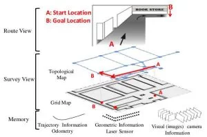
What is LPKF?
LPKF is a group of machines that produce printed circuit boards (PCBs). PCBs are used in practically all electrical devices, and the Process section below details all of the stages involved in creating a PCB.
Process
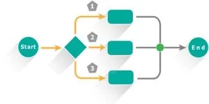
The list below provides a general overview of all the stages involved in creating a PCB. The LPKF technique allows us to create boards with up to eight layers; nevertheless, two-layer boards are far more typical.
Materials

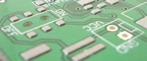
The most commonly utilised material for pcb manufacture is FR4. A top layer of copper, a middle layer of fibreglass, and a bottom layer of copper make up this structure. The circuit board is then drilled and routed away from the material.
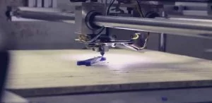
Drill Through Holes
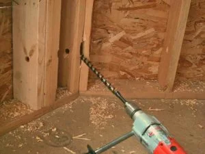
The first step is to drill all of the through holes, also known as vias, on a blank sheet of FR4. A via is a hole in the upper layer that links to the lower layer. These are frequently used to connect ground planes on the top and bottom levels, preventing capacitive effects between them. Vias can also be used to move a trace from one layer to another, which can be useful for avoiding conflicting traces.
Plate Through Holes
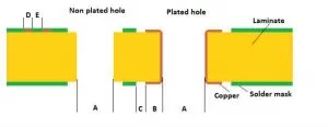
The vias that were recently drilled are plated, adding a thin layer of copper to them. This is what connects the top and bottom layers.
Route Top Layer
The boards are then returned to the router, where the top layer’s tracks are routed. The tracks on a PCB connect all of the components together.
Route Bottom Layer
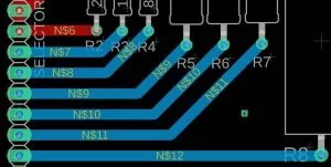
The boards are then flipped over and the bottom layer is completed in the same manner.
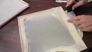
Apply Solder Mask
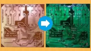
The solder mask is what gives most PCBs their green colour. It has two purposes: 1. Protects the board by acting as an insulating layer on the top and bottom, and 2. repels solder. The solder repellent characteristic makes soldering components that are close together or have pins that are near together much easier. Because of the solder mask, solder is less likely to bridge across pins.
Apply Silk Screen
The silk screen is quite similar to the solder mask. The same procedure is followed, except this time the board is white and text is printed on it. Text can comprise anything from component labels to corporate logos to board dates of manufacture.
Route Stencil
Solder paste is applied with the use of stencils. A stencil is a polyimide sheet with holes cut in it that correspond to the pads on the board’s components. The stencil is routed similarly to the boards in this system.
Apply Solder Paste
The LPKF system includes a jig that helps align the stencil with the board and makes solder paste application easier.
Place Components
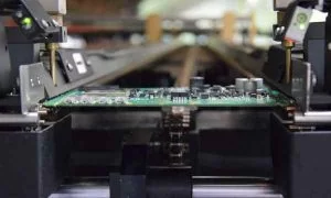
After the solder paste has been deposited, all components are placed on the board using a pick and place method.
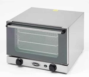
Reflow
A reflow oven is essentially a sophisticated toaster oven that warms up to the point where solder melts but not hot enough to harm the board. The board is finished after reflowing.
Equipment
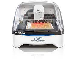
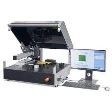
Protomat S64
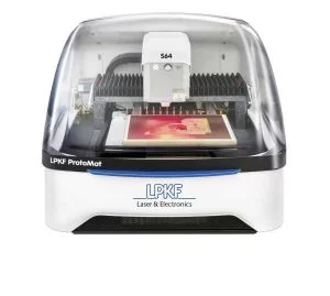
The board router is the ProtoMat. This equipment is used to drill and route the PCB as well as create stencils for solder paste application.
Circuit Pro
This is the CAM software that is used to build up tasks and control the S64.
Contac S4
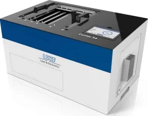
This is the copper plating vias through hole plater. There’s also a setting for tin plate pads that makes them look silvery instead of coppery.
ProMask
To apply the solder mask, you’ll need a solder mask kit.
ProLegend
Silkscreen graphics are applied with the use of a silkscreen kit.
ProtoPlace
Machine for picking and placing items. It is used to pick up and position components on the board. This is far more convenient than doing it by hand.
ProtoPrint
The stencil is aligned to the board using this jig. Solder paste may be simply applied to all of the pads from here.
ProtoFlow S N2
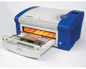
This is the reflow oven, which is used to heat the circuit board to the point where the solder melts. It’s also used to cure the silk screen and solder mask.
Terms
PCB stands for “Printed Circuit Board.”Surface Mount Device/Surface Mount Technology (SMD/SMT) (components that attach by being soldered to pads on one side of the board)
The term “through hole” refers to a hole that runs the length of the board.
Trace/Track – A trace/track is a circuit board wire that connects one component to another.
Fiducial – Holes used to track and pick up the board’s position.
Mask for soldering
Silkscreening