Summary of PIC32 DMA Graphics with Single Frame Buffer ECE 4760 Final Project
This project demonstrates Direct Memory Access (DMA) on a PIC32 microcontroller for graphics and external memory operations. The team built two demos: transferring data to a TFT display via SPI and reading from an external RAM chip using DMA, aiming to offload CPU tasks for high-performance graphics.
Parts used in the PIC32 DMA Graphics Project:
- PIC32 microcontroller
- TFT display
- SECABB v2 board
- External RAM chip (23LC1024)
- SPI controllers
- DMA channels
- Data/command select wire
- DM74LS08 AND gate
- SN74AUC1G08 AND gate
Introduction
For our final project, we created two demonstrations utilizing direct memory access (DMA) in a graphics setting. Our original intent was to implement the video game DOOM on the PIC32, however that proved to be an undertaking too large given the time constraints of the project. Our preliminary exploration of implementing DOOM on the PIC concluded that there would be performance and memory constraints if a direct port was created. To solve this problem we decided to look into implementing a frame buffer for the PIC32, which would serve as a way to store all of the draws done to the TFT in various passes in a single location and would enable the PIC32 to start calculating the next frame to be displayed while the TFT was still drawing the current frame.
Due to the complexities involved in utilizing DMA, our original plan had to be trimmed down. Nonetheless, we were able to create two demonstrations of DMA that can be further expanded upon to create complex, high-performance graphics and animations on the PIC. First, we were able to show DMA moving a data array on the PIC32 to the SPI buffer of the TFT. Our second demo involved enabling the DMA controller to perform reads from a RAM chip. Much of the work done for this project could be considered “exploration,” as we had to dig deep into the reference manuals and create a unique system.
High Level Design
The eventual goal of this project was to implement a frame buffer that could, independently of the CPU, copy its state to the TFT. This would require the use of an external memory that could hold enough data to store 16 bit color for every pixel of the TFT at the desired resolution. The size of a single frame buffer for the TFT at the native resolution of doom (320 x 200) would take up 128 KB of RAM, much more than the PIC32’s 32 KB. Another benefit to the use of the external frame buffer was the reduction in the number of commands required to control the TFT. Normally, a draw to the TFT requires that there are 7 transfers done to the TFT before anything else can be drawn, but by utilizing the TFT’s behavior of wrapping the location written to if you write too much data, we were able to continuously write to the TFT without any extra commands.
The TFT communicates to the PIC32 using serial peripheral interface (SPI). SPI interfaces have 4 wires, 3 of which can be shared between any number of peripherals. The 3 shared wires are clock, master out slave in (MOSI) and master in slave out (MISO). Each peripheral also has an independent chip select line from the SPI master. Most of the wires are generated by the SPI master. In the case of the PIC32’s SPI controller acting as SPI master in its default mode, the SPI clock signal will only be generated when the controller is transmitting data to one of the peripherals. Likewise, the SPI controller will only read from MISO when it is sending data over MOSI.
The Direct Memory Access (DMA) channels are complex pieces of hardware which utilize the PIC32’s internal memory bus to directly copy memory from one location to another when activated by the CPU or some interrupt, including those generated by peripherals. Due to the PIC32’s peripheral devices being memory mapped, the DMA channels can easily interact with all PIC32’s peripherals. Several DMA channels can be triggered by a single interrupt and to decide which order the DMA channels run in, the DMA controller utilizes DMA “priority.” If not modified, DMA channels with a lower id will run before DMA channels with a higher priority (DMA 0 would run before DMA 1), though for long transfers they will sometimes alternate running. If the priority of the DMA channels is modified, DMA channels with a higher DMA priority will take absolute control over the memory bus, blocking the other channels until the higher priority channel no longer needs the channel.
Our design was supposed to have two RAM chips that were mapped to one of the PIC32’s SPI channels. The RAM chips would be used to store a frame buffer, which the PIC’s DMA channels would send to the TFT via the SPI channels on the PIC32. By offloading the writing of the frame buffer to the TFT, we would expect that the PIC32 could more easily keep up with the timing that would be needed to run DOOM. While the CPU is calculating the pixels for the next frame on one RAM chip, the DMA would be writing the current frame, on another RAM chip, to the TFT without needing to interact at all with the CPU.
Design
DMA TFT Graphics
Hardware
The TFT and PIC32 are already connected together on the SECABB v2 board, with the board traces linking the B0, B2, B11 and B14 pins on the PIC32 to the TFT as well as providing independent ground and power (Appendix D.1). The TFT’s chip select line also has an exposed jumper that is normally linked to the PIC32’s B1 pin. The main communication protocol between the PIC32 and the TFT consists of a standard 4 wire SPI interface, along with power, ground and a special wire called data/command select. The special data and command select wire allows the SPI master to control how the TFT interprets the received data. For the hardware on the PIC32 side, there are 2 important hardware peripherals, the SPI controllers and the direct memory access (DMA) channels. For the hardware on the PIC32 side, there are 2 important hardware peripherals, the SPI controllers and the direct memory access (DMA) channels.
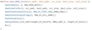
The most important feature of the DMA channels that we use in this project is the ability of a DMA channel to interface with and write data to change the behavior of another DMA channel because the DMA channel settings are mapped to a location in memory since it is a peripheral. Using this idea and previous work done by Bruce Land and Joseph Primmer (Appendix C, DMA Weird Machine), we were able to construct a rudimentary DMA processor, also called the DMA weird machine, which took instructions from memory and wrote them into the control registers for a different DMA channel which would then execute them. Each DMA instruction consists of the state of multiple different control registers for some DMA channel. We call each instruction a DMA block, as it consists of a block of control registers. The DMA block instruction contains the size of transfer, the address of the source and destination, and their respective sizes. It also contains the id of the interrupt that will cause the channel to trigger a transfer, usually the executing channel triggers when the fetching channel has completed its transfer. However, if the execution is not triggered off of the fetching channel finishing its transfer, it is important that the executing channel be placed at a lower priority, to ensure that the execution doesn’t occur before the fetching channel finishes loading the instruction.
Since all the instructions in the DMA processor are exclusively move operations, it makes understanding the program extremely difficult even when compared to assembly. For example, a simple task like branching, takes at least 4 instructions, and needs a lookup table in memory to determine the result of the branch operation. The value is read into the lowest byte of address of the lookup table that holds pointers to the locations for the next instruction to execute. The pointer (next_read_addr) is then read into the address field of the instruction 2 blocks ahead of the executing block. The next block modifies the channel that is fetching the instructions so that it will now fetch from next_read_addr and continue executing the DMA program from there.
The final detail of the DMA weird machine is that the instruction cycle time is dependent on the size of the transfers completed. The DMA blocks that we utilize are 132 bytes in length because this length allows us to change the interrupt that the executing DMA channel is triggered off of, on the fly. The reason why the block size is so big is because each DMA channel has 3 shadow registers along with the default register which can set, read the inverse, and clear the selected bits. These operations are also memory mapped in between each control register which results in the DMA blocks taking up much more memory than one would initially expect.
The PIC32 has 2 SPI controllers to go along with the 2 SPI channels that are available on the PIC32. The controllers also handle the data interaction between the other parts of the PIC32 and the SPI channel. The main part of the SPI channel’s data interface is the SPI Buffer. In the default mode, this buffer consists of a 32 bit register which, when written to by the CPU, will initiate an SPI transaction which will send 8, 16, or 32 bits of data from the buffer and into the data lines, depending on which mode that the SPI controller is in. The result, which is received simultaneously, is then written into the SPI buffer.
There are multiple other modes for the SPI controller but the most relevant one for this project is Framed SPI mode. In Framed SPI mode, the SPI controller takes as much control as it can away from the CPU. This means that the SPI controller will now control the chip select line automatically. It also makes the SPI clock run continuously, whereas in normal mode the SPI clock only runs when there is a transfer actively happening. This basically means that the SPI controller is set up to interact with a single peripheral. The reason why this mode is important is because this is the only mode that a DMA channel can cause the SPI controller to write to the SPI channel. In all other modes, the SPI controller doesn’t respond to the DMA channel’s write.
The usage of framed mode necessitated a change in the hardware configuration that is normally used on the SECABB v2 board. The TFT_CS pins which are usually connected with a jumper were disconnected because the chip select line was now connected to the SPI controller and could only be mapped to a different output pin, which necessitated running a wire to connect the TFT_CS line to the B3 pin on the board. Pin B3 was mapped to the chip select line generated by the SPI controller (SS1) through the PIC32 peripheral pin select muxes (PPS).
The most important configuration for our usage of framed SPI mode (enabled with the SPICON_FRMEN option) on the PIC32, was the configuration of the SPI controller’s generation of chip select (CS). There are a number of options to control how the chip select is generated, the polarity of the CS (active high or low), the length of the CS and the triggering of CS relative to the first bit of data sent from the SPI controller. The TFT cannot have the CS constantly held in active low because it results in the TFT basically never updating. For the TFT, the required framed mode settings were:
- Setting the polarity to active low (default)
- Setting the generated CS pulse to be aligned with the first bit of the transfer (SPICON_SPIFE)
- Setting the generated CS pulse to be 1 word length wide (SPI_OPEN_FSP_WIDE)
- Length depends on which mode the SPI controller is in (8, 16 or 32 bit width pulses possible)
Software
The tft_master.c (Appendix F) file provided in the course contains the graphics functions needed to draw to the tft. Of particular interest was the tft_drawPixel() function, which draws a pixel at a specified coordinate. The underlying structure for this entails calls to the tft_writecommand() function, followed by calls to the tft_writedata16() function. To draw a pixel, the code first wrote the column address set (CASET) command to signify a column coordinate. Next, the x and x+1 coordinates would be written. A similar structure was also used for the row as well as the color value. The drawPixel() function utilizes the TFT’s range selection features to select a single pixel and draw a single piece of data to it. By selecting a larger section, the PIC32 could draw to any arbitrary rectangle on the screen by modifying which x and y coordinates it draws to, The original plan was to model the pixel drawing sequenece using DMA, and then transition to vertical line drawing, as that would be the method we would use in drawing an entire screen.
Since these SPI writes are all written to the TFT buffer, we decided that we could mimic this structure using DMA. The DMA weird machine code developed by Bruce Land creates macros, or blocks, which copy the control register states for a DMA channel into a stack-allocated array which is used to create a DMA instruction (Figure 1). This standard way of creating a memory transfer block allows for us to specify where a chunk of memory is to be moved to, and how much is sent in a single transfer. In this macro, we can also specify when a block is supposed to start performing a transfer. By instantiating multiple DMA blocks with different input parameters, larger programs can be made. Using these DMA blocks, we worked to mimic the movement of data to registers in the same way as the tft_master.c code.
Unfortunately, after weeks of debugging, we were able to simulate the two commands but the commands didn’t seem to draw anything on the TFT. We were even able to execute an arbitrary series of the two commands but that didn’t translate that into the drawing actually being shown on the PIC32. In our debugging, we were able to confirm that our program structure was correct and that memory moves were happening by printing relevant variables to the TFT. Here we were essentially able to execute any function based on an array of function pointers. We also realized that this structure would not be practical because we would easily fill up the memory constraints of the PIC with the massive data structures needed to complete this design. Each extra loop through the DMA program would have required approximately 20 bytes of memory. Considering that the DMA program would likely have to be at least 200 instructions long (one for every pixel in a vertical line drawn for the TFT resolution that we would be using), we would have needed around 35% of our available RAM space just to store the data needed to execute this method.
Initially, we also wanted to specify the creation of the drawing address window via DMA, however that was not able to work, as we ran into the same problems mentioned above. We initially thought that our graphics weren’t working because this function was not being done correctly in DMA. However, even when reverting the address window initialization back to its tft_master.c form, we still encountered issues. Nonetheless, to reduce the number of moving parts, we decided that we could leave the tft_setAddrWindow() call as is because this only happens once at the start of the program.
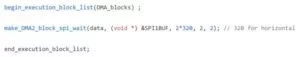
Going back to the drawing board, we ended up creating a simpler structure that would directly write an array to the TFT’s SPI buffer (Figure 2) (See DMA_TFT.c in Appendix F). This approach allowed us to draw pixels to the TFT based on the contents of a 320 element data array which stores pixel colors. The one downside of this approach is that it can only draw vertical lines. Since there is no way to specify rows or columns, each element in the 320 long array represents the color for the entire column. The make_DMA2_block_spi_wait() DMA block is created with the same macro as in the DMA weird machine (Figure 3). Here, we specify the block transfer to begin on the _SPI1_TX_IRQ. This IRQ signifies the completion of an SPI transfer. In our code, whenever all 320 elements in the data array are written to, the DMA block will initiate the transfer of this data into the TFT’s SPI buffer, which will result in colors being drawn on the screen. With the DMA channel active, the TFT would be updated every time the 320 element data array was defined.
DMA RAM Chip
Hardware
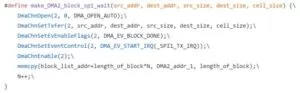
Having learned that we needed to get the SPI channel used to communicate with our peripherals running in framed mode working for our DMA channel to interact with the peripherals, we looked into implementing framed mode for our interactions with the RAM chip. The issue we immediately encountered was evident when looking at the chip select signal required, when reading data from the RAM, which can be seen in Figure 4 below.

As discussed when talking about framed mode for the TFT, the framed mode SPI channel can only lower the chip select line for 8, 16, or 32 bits, much shorter than the number of bits that we need if we are transferring enough data to fill a 320 pixel data array. We also discovered that the read would fail if chip select (CS) was ever raised during the read. To solve this problem, we decided that we would not use the CS generated by the SPI controller (referred to from now on as SS2) and instead use our own CS line generated from the GPIO controller.
However, this solution introduced another problem. Since the SPI clock (SCLKx) is always being sent by the SPI controller when the SPI channel is running in framed mode, the RAM chip would constantly be receiving clock signal while the chip select was held low and so the RAM chip would interpret the inactive MOSI line as data being sent from the PIC32, since the clock was running and CS is held low. Both the PIC32 and our DMA processor are not fast enough to lower CS and immediately start a data transfer in the same SPI clock cycle. This means that the RAM would incorrectly read the data sent on the SPI channel from the PIC32 as shifted by a large number of bytes which means that the read command would fail and the RAM wouldn’t send the expected response. The only solution with that SPI setup would be to decrease the SPI clock frequency to be slow enough that the DMA processor can trigger a transfer before the next clock cycle, which would lose much of the speed benefits that the frame buffer gains.
The solution that we thought of to use the RAM in framed mode was to make framed mode behave like the PIC32’s default SPI mode. We had already progressed in this direction by not using SS2 and using a GPIO generated CS. The only change we would need to make to the framed SPI mode signal behave like the default SPI mode would be to have the SPI clock only run when there is a transfer occurring. Since SS2 can be configured to be active high only when there is a transfer occurring, using a logical AND gate between the SCLK line and the SS2 would result in the RAM chip receiving an SPI signal as if the PIC32’s SPI channel was in its default mode of operation. The diagram D.2 in Appendix D, shows the configuration of the signals sent between the PIC32 and RAM.
The configuration of the SPI mode for this setup was slightly different from those used to interact with the TFT because SS2 needed to be active high to let the SCLK control the signal when there was a transfer occurring. The SPI configuration settings were:
- Setting the polarity to active high (SPICON_FRMPOL)
- Setting the generated CS pulse to be aligned with the first bit of the transfer (SPICON_SPIFE)
- Setting the generated CS pulse to be 1 word length wide (SPI_OPEN_FSP_WIDE)
- Length depends on which mode the SPI controller is in (8, 16 or 32 bit width pulses possible)
This configuration let the provided SPI RAM software function in framed SPI mode, though there were still some bugs. The main bug was that when we read from the RAM chip, the PIC32 returned a value one half the value that we expected. This seemed to indicate that the PIC32 was reading an extra bit before the RAM was sending data. Because the PIC32’s SPI controller can only send and receive data in byte length packets, we eventually determined that the SPI RAM was sending data much later than the PIC32 was reading the data. We could confirm that this was the case because when we decreased the SPI clock speed from 20MHz to 2 MHz we found that this bug disappeared and that the RAM chip functioned exactly as expected.
Further investigation with an oscilloscope led to the conclusion that the SPI RAM’s SCLK was delayed by about 30% of the clock period with the SCLK sent by the PIC32 when running at 20 MHz. The reason for this was that our initial logical AND gate was the DM74LS08 had a propagation delay which was a significant fraction of the SCLK cycle time. The SCLK was running at 20MHz, which meant that it had a period of 50 ns, with a 50% duty cycle square wave. The AND gate had a proportional delay of about 13-18 ns which meant that the RAM was receiving the clock approximately half a cycle after the PIC32 sent it. This was barely enough to let the SPI RAM receive commands but meant that the PIC32 sampled the MISO line before the RAM could set up the clock line.
The solution to this problem was to purchase a significantly faster AND gate which had a setup time that was much fatter than the cycle time. The product that we purchased was the SN74AUC1G08, a high frequency AND gate which had a propagation delay of at most 2 ns, less than a 20th of the clock cycle. Substituting the new AND gate for the DM74LS08 and running at 20 MHz clock rate resulted in the expected behavior of the SPI chip. The physical implementation of the RAM and AND gate circuit is shown in Appendix D.4
Software
In terms of software, we first made sure our RAM chip setup worked by using the Uart_spi_RAM_DAC.c example provided on the course webpage (our modified code is found in Appendix F). With a PUTTY terminal active, this code allowed us to send different commands to the RAM chip such as reading, writing, as well as reading an array of values, among others. The read commands printed their output to the terminal, which was essential for verification. Once we understood how to operate this code, our next task was to extend its functionality such that we could perform memory operations using DMA. Starting with getting byte reads working with DMA, we had to forgo the typical DMA block structure of the DMA weird machine as we needed greater control of the individual function calls that make up the macro.
The DMA structure we devised starts with a DMA channel sending the read address to the RAM chip, and reading the junk response. After this, we use three DMA channels to complete the read. One channel writes junk to the SPI2BUF to force the SPI channel to read incoming data from MISO as well as generate clock signals to send to the RAM. Another channel reads the data from the SPI2BUF of the RAM chip into the output array. The last channel is used to clear the interrupt from the channel that is reading from the transfer buffer, so that the channel that writes junk can be triggered multiple times. Once completed, we needed to disable the three DMA channels we used because one channel is used for printing to UART, and the other two channels we do not want to get accidentally triggered outside the DMA read function. This action allowed us to preserve the DMA state while running the DMA program. When defining the operations of these DMA channels, we needed to take extra precautions regarding UART and SPI communication. Specifically, we added NOPs before initiating the actual reading so that the CPU wouldn’t print a response to the UART terminal before the response was read from SPI.
Results
Here is a link to our demo, showing the results of our project: Demo
The final output of our project was two demonstrations of DMA used on the PIC32. The first demo showed the TFT being drawn via DMA data transfers to the TFT’s SPI buffer. To visualize this, we created a sequence which updated the 320 element array with different colors. A video of this can be seen below in Figure 5.
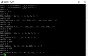
The second demo had DMA channels set up to read from a RAM chip. A sample terminal output can be seen below. The ‘w’ command is the write byte command, the ‘r’ command is the read byte command, the ‘d’ command reads a series of bytes through DMA.. Upon initialization we set the value of each memory address to itself modulo 256 so that we have expected values.
Conclusion
In terms of our expectations, we definitely had to lower them on multiple occasions as we discovered more and more fundamental constraints with the systems with which we were working. Next time, we might consider attacking the project in a different manner. Perhaps by starting with work on the game instead of the graphics optimizations. Optimizations are normally something you want to focus on after getting a working base functionality. So, perhaps, instead of anticipating what optimizations we might implement before we should have worried about them, we could have focused on just getting the game to start running on the PIC32.
With consideration of intellectual property, we need to consider that we used code which was designed by others. The first of these is the DMA Weird Machine, created by Bruce Land. The second of these is the UART SPI RAM code, also made by Bruce Land. The last of these is the TFT draw code, originally written by Limor Fried and subsequently rewritten by Syed Tahmid Mahbub. In our original plans to port DOOM, we would have used the open-source code that is available on GitHub. Since we did not end up porting DOOM, we did not use that code base. However, we still included it in our Appendix C for interest’s sake. Despite using much open-source code, we do not use code in the public domain. We don’t really see many patent opportunities for the project, and there does not seem to be many opportunities for publishing either. However, this project provides a great infrastructure for someone to develop complex, high performance graphics with. If someone were to expand upon this project, patent/publishing opportunities may arise. Nonetheless, for someone who wants to really dive deep into DMA and SPI on a PIC32, this project could be of great interest and use.
We don’t really see any ethical considerations here. There is nothing done in this project that could put anyone in serious and immediate danger if something went wrong. Diving deep into DMA is unlikely to lead to any future technologies that would be of ethical concern, either.
Besides typical lab safety, there are really no safety concerns. Most of our project was based on hardware interaction inside the PIC32 and the external hardware we did was simple breadboard wiring, which had a maximum voltage of 3.3 V and maximum current around 10 mA.
In terms of any legal considerations, we really only have to worry about using other people’s open-source code. Because of this, we would have to consider the implications of that before doing anything with our own code.
Overall,this project was a great experience for us and we most certainly got a lot of experience working with low-level programming and hardware interaction on the PIC32.
Source: PIC32 DMA Graphics with Single Frame Buffer ECE 4760 Final Project
- Why was the original DOOM port plan changed?
The team found performance and memory constraints that made a direct port too large for their time limits. - How does the frame buffer improve performance?
It allows the PIC32 to calculate the next frame while the TFT draws the current frame without CPU interaction. - What hardware configuration is required for Framed SPI mode with the TFT?
The TFT_CS jumper must be disconnected and wired to pin B3 to allow the SPI controller to manage the chip select line. - Why could the DMA weird machine not draw pixels directly?
The massive data structures needed would consume approximately 35% of the available RAM space. - How did the team solve the chip select issue when reading from the RAM chip?
They used a GPIO generated CS line instead of the SPI controller's SS2 line and added an AND gate to control the clock signal. - What caused the initial read errors from the RAM chip?
The DM74LS08 AND gate had a propagation delay that caused the PIC32 to sample data before the RAM was ready. - Which component solved the timing issue with the RAM chip?
A faster SN74AUC1G08 AND gate with a propagation delay of at most 2 ns resolved the synchronization problem. - What is the maximum resolution supported by the single frame buffer design mentioned?
The design targets the native resolution of DOOM which is 320 x 200 pixels.