
Summary of PIC16F877 Development Board v. 1.2
The Development Board v1.2 is a versatile PIC16F877/16F874 evaluation board providing configurable clock (RC or crystal), in-circuit programming connectors (including LVP support), octal LED buffer for monitoring up to 8 I/O lines, double connectors for all MCU pins, dip-switch selection for modes and LVP, trimmer for A/D input, reset options, onboard 5V regulator or external supply, and status LEDs. It is double-sided, modular for partial assembly, and intended to ease hardware/software development and in-circuit programming without removing the PIC.
Parts used in the Development Board v1.2:
- PIC microcontroller (PIC16F877 or PIC16F874)
- Crystal oscillator (1 MHz to 20 MHz) and crystal connector
- RC network for clock (resistor and trimmer capacitor)
- Trimmer potentiometer (for A/D input)
- Octal CMOS buffer (driving eight LEDs)
- Eight small LEDs for I/O monitoring
- Double connectors for MCU pins (plugs and wires)
- Connector for programming cable
- Dip switches (4-, 6- and individual switches for pin selection and LVP)
- Reset switch
- Components for RESET pull-up and RC Power-On circuit (resistor, capacitor)
- On-board 5V regulator (with input capacitor and regulator components)
- Power supply components (input jack, smoothing capacitors)
- LEDs indicating supply presence (up to three)
- PCB double-sided board (with silkscreen)
- Various passive components (resistors, capacitors, headers)
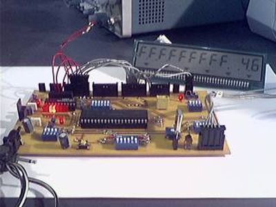
The Development Board v. 1.1 connected to an LCD display. It is well visible (read further, in the description) the row of LEDs used to check the logic state of up to 8 I/O ports or external circuits’ pins. Of course, if you own an 8 trace oscilloscope, you can do without it. :-)) On the right bottom the programming cable.
Characteristics of the DB12
As I have done with the PIC 16F84 / C84 Evaluation Board, designed and built by myself according to my need, when approaching a higher level microcontroller I decided to design a circuit allowing easy development of applications. This board, in fact, allows the PIC to be interfaced with external circuits in a reliable and versatile way, making it possible to blame just the external circuits in case of electrical problems, and, of course, to concentrate just on the software.
Supported microcontrollers: PIC 16F877, 16F874
Note: the PIC 16F877 pin-out is upwardly compatible with the pin-out of PIC 18F442, 18F452, 18F448, 18F458. This board have been designed for PIC16F877 and tested with it (and on this page we’ll always refer to it); the circuit should be anyway suitable for mentioned microcontrollers, too (18F4x2 and 18F4x8), with the following notes:
a) the OSC2 pin would be multiplexed with RA6
b) in the 16F877, LVP programming and LVP-mode working involve the RB3 pin, while in the 18F4x2 and 18F4x8 families the RB5 pin is involved, so, in these ones, the LVP mode is not selectable just through a dip-switch like you can do for the 16F877; LVP working (but not LVP programming) should be anyway possible connecting to the ground the proper pin, through a resistor, through the board’s connectors or through a wire
c) the values of capacitance adviced for the main crystal oscillator, in the range 1 MHz to 20 MHz, are the same in the datasheet of the 16F877 and of 18F4x2 and 18F4x8 families; the value of 15 pF choosen for this board (and tested with crystals from 4 MHz to 20 MHz with the 16F877) should therefore be suitable also for the two mentioned 18 families.
Let’s now describe the main characteristics of this circuit:
- Clock generated by RC net or by crystal (XT,HS); clock frequency can be varied with a trimmer in RC mode and using different crystals in the XT and HS modes (without soldering them, but just inserting them into a connector)
- Octal CMOS buffer driving eight small LEDs: you could connect to the buffer’s inputs, by convenient but affordable wires (red wires in some of the pictures above), PIC’s I/O pins and pins of any external circuit (external circuit and this board connected to the same ground reference), and you can do this without charging the sources; of course, signals being monitored can be carried to other points through another connector
- Double connectors, both for plugs and for wires, to connect to the external world all the microcontroller’s pins (RESET and supply included)
- Connector to connect the PIC to various kinds of programmers, allowing you not to remove the PIC from its own socket. NOTE: THIS BOARD IS NOT A PROGRAMMER.
- LVP mode selected through a dip switch
- Selection of working modes through 4 or 6-ways dip switches
- Trimmer to experience on-chip A/D converters (you can connect it to any of the 8 A/D converters of the 16F877)
- Reset switch; selection of connection of RESET pin to Vdd through a simple pull-up or through a RC Power On circuit; the RESET pin can be driven by a programmer or by external circuits
- Supply modes: 5V sourced by the on board regulator (input about 7-15V), that can also be fed to external circuits, or supply to the PIC from external circuits
- LEDs signaling presence of supply in different points of the board (you can disconnect one of the three LEDs)
As previously said, this circuit is not a PIC programmer, but it can be easily interfaced with one of the many programmers you can find, allowing you not to remove the microcontroller from the board (in-system programming).
Compared to the version 1.1, connection also to LVP programmers is now supported; besides this characteristic, it is of course possible to work both with chips with the LVP bit set (just a switch need to be set) and with the LVP bit not set; it is of course possible to interface the board with traditional programmers (12 V on /MCLR), the most part, I would say.
The D.B. is built on a double side board, so realizing it is not the simplest thing in the world; besides, taking a look at the layout, you can easily recognize that it was the only way to make it, unless one had decided to insert dozens bridges.
NOTE: the images of the layout and the schematics further on this page are at low resolution, for obvious problems concerning the time needed to load this page, but their links point to better resolution images. When you click on a link of an image (i.e. the layout) and a new window opens, I suggest you not to close it, as it could be useful to take a look at it while reading this page and in particular for the examples that are further described.
While designing this circuit I tried to realize a versatile circuit and, in the same time, I also pursued the possibility to mount only the components one wish, making this D.B. a not expensive one.
It is of course possible to mount later a part or all the components not soldered at first.
The version here described is the 1.2, completed in February 2003.
Images needed to realize the circuit
If you wish to realize the Development Board (after reading, in particular, the “Acknowledgement and disclaimers” section), you can find here the links to save the images you need (at 300 dpi), reachable anyway in other points of this page. Advices for printing in the layout printing section further.
Copper side layout at 300 dpi (316 KB)
Components side layout at 300 dpi (178 KB)
Components placement (silkscreen) at 300 dpi (131 KB)
Electrical schematic at 300 dpi (240 KB)
Components placement and track view at 300 dpi (465 KB) , or, still good quality,
Components placement and track view at 200 dpi (251 KB)
Why so many dip-switches?
I have choosen to use a switch for each pin that sometimes has to be insulated or connected to other particular pins (i.e., during programming), both to grant a safe insulation and because using 3-state buffers could not be so easy and they could have some electrical problems (i.e, /RESET and supply).
In any case, during the normal switch between use and programming, as an example when the software is being developed, to allow the chip to be programmed it is usually enough to carry out a few simple operations, not more than a few seconds, setting to OFF some switches of a few dip switches and those of another dip-switch to ON (others dip-switches can be left as they are). As soon as the chip is programmed, it is enough to carry out the inverse operation so having the PIC ready again and connected to the external world. In the section “Programming” operations to carry on are reported in details for the various kinds of programmers, their supply and the LVP bit of the PIC.
For more detail: PIC16F877 Development Board v. 1.2
- Which microcontrollers does the board support?
The board is designed for PIC16F877 and PIC16F874 and is compatible with PIC18F442, 18F452, 18F448, 18F458 with noted differences. - How can the clock be provided to the PIC?
The clock can be generated by an RC network with a trimmer or by inserting different crystals (XT, HS) into a connector. - Can the PIC be programmed without removing it from the board?
Yes, the board has a programming connector allowing in-system programming; it is not a programmer itself but interfaces with programmers. - Does the board support LVP programming?
Yes, version 1.2 added support for LVP programmers and LVP mode can be selected via a dip switch for the 16F877. - How are I/O signals monitored on the board?
An octal CMOS buffer drives eight small LEDs to monitor up to eight I/O pins or external circuit pins. - What supply options are available?
The board can supply 5V via an on-board regulator (input 7–15V) or the PIC can be powered from an external supply. - How are pin connections to external circuits provided?
Double connectors for plugs and wires provide access to all microcontroller pins including RESET and supply. - Can the RESET behave as power-on RC or simple pull-up?
Yes, RESET can be tied to Vdd via a simple pull-up or via an RC Power On circuit, selectable on the board. - Are all components required to be soldered at once?
No, the board was designed so you can mount only the components you wish and add others later. - Why were so many dip-switches used?
Individual switches per pin allow safe insulation or special connections (e.g., during programming) without complex 3-state buffers.
