


Summary of PIC12CE518 I2C EEPROM using PIC12CE518 with Proteus Simulation
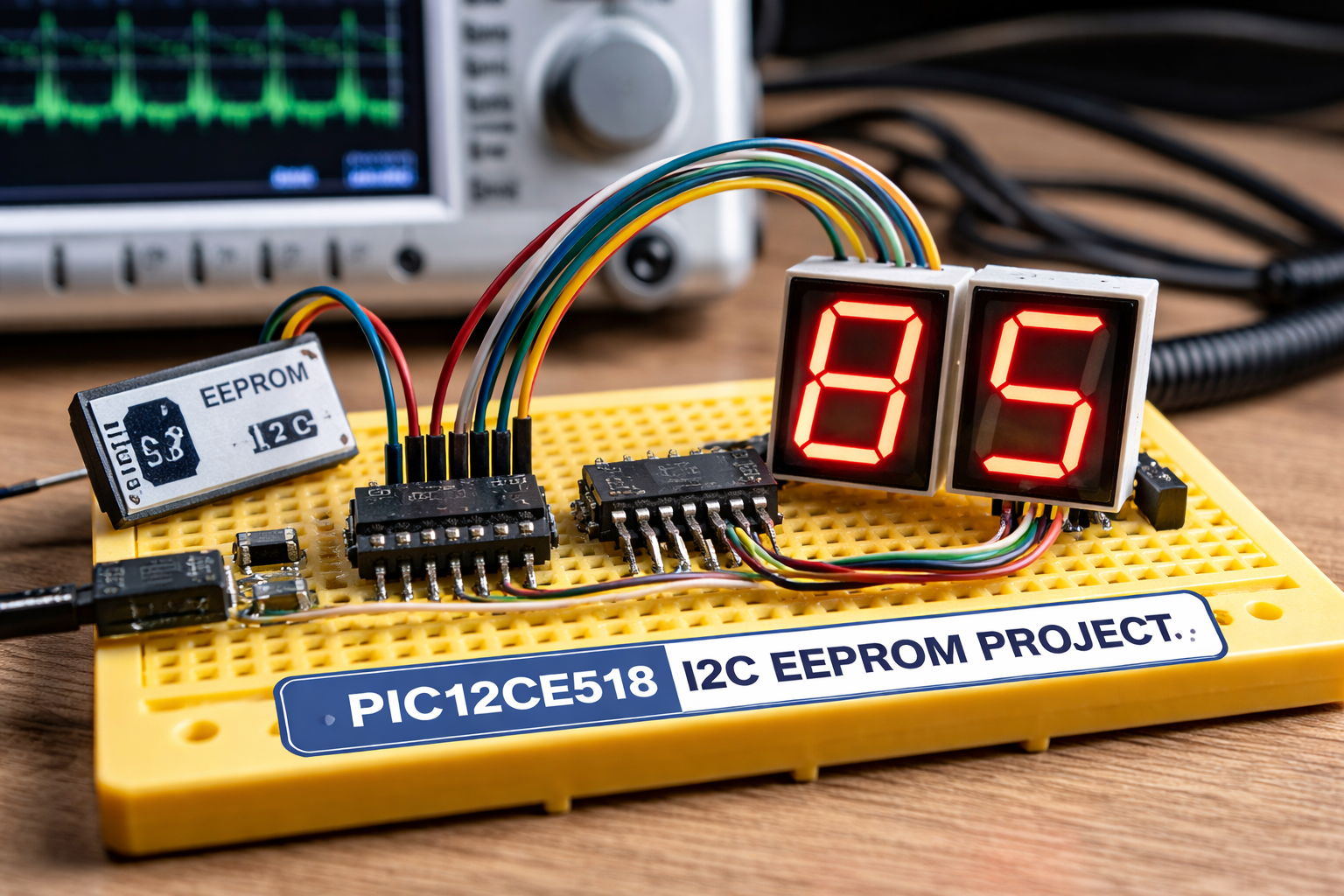
This article details a PIC12CE518 microcontroller project demonstrating internal I2C EEPROM read/write operations. The system writes the value 0x85 to memory, reads it back, and displays the data on 7-segment screens via a shift register using serial GPIO transmission. Simulated in Proteus, the project serves as an educational tool for understanding embedded memory management, firmware handling, and real-time data visualization in compact microcontrollers.Parts used in the PIC12CE518 I2C EEPROM Project:
- PIC12CE518 Microcontroller
- 74199 Shift Register
- 7-Segment Displays (2 units)
- GPIO-based input trigger
- Power supply
- Proteus VSM simulation environment
Introduction
This microcontroller project demonstrates how to write and read data using the internal I2C EEPROM of the PIC12CE518 and visualize the result through digital outputs. Designed and tested in Proteus simulation, the project highlights practical EEPROM interfacing—an essential concept in embedded systems and DIY electronics.
The system writes a value (0x85) into EEPROM memory, reads it back, and transmits the result serially for display. This makes it a great learning example for understanding data storage, I2C communication, and firmware handling in compact PIC microcontrollers.
This PIC12CE518 EEPROM Proteus Simulation also helps reinforce how EEPROM operations work in real embedded system applications.
How the Project Works (Overview)
The project revolves around the internal EEPROM module of the PIC12CE518. The firmware performs a continuous loop of operations:
Initializes GPIO pins for communication
Writes a fixed byte (
0x85) into EEPROMReads the stored value back
Sends the value serially via GPIO pins
Waits for input signal transitions to repeat the process
The EEPROM operations use built-in routines (WRITE_BYTE, READ_CURRENT) from Microchip’s EEPROM driver.
Workflow Explanation
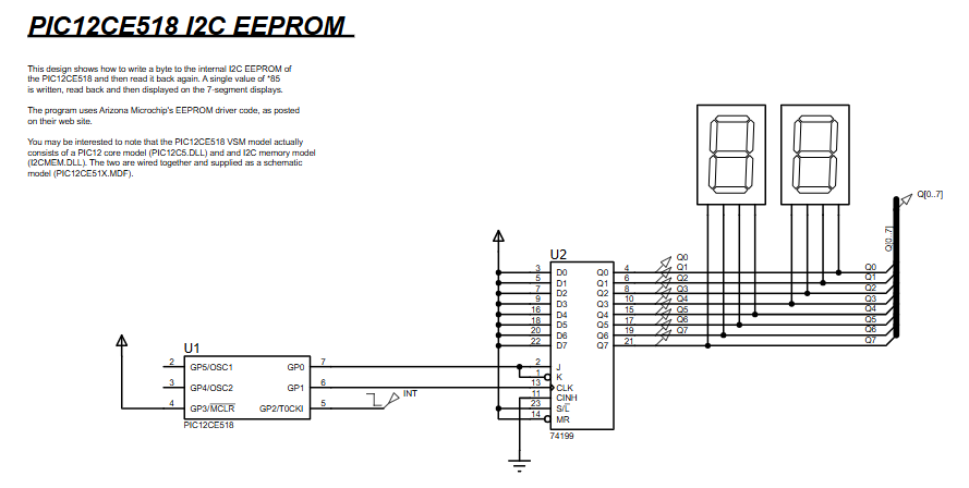
Based on the schematic and code logic, the workflow is:
PIC12CE518 Controller
Controls EEPROM operations
Manages GPIO communication
Internal EEPROM
Stores the byte value (
0x85)Address pointer increments each cycle
Shift Register (74199)
Receives serial data from PIC
Converts it into parallel output
7-Segment Displays
Display the stored EEPROM value
Input Trigger (GPIO Pin)
Controls timing for read/write cycles
Workflow Steps:
Write → Wait → Read → Output → Increment Address → Repeat
Key Features
Internal I2C EEPROM read/write implementation
Serial data transmission via GPIO (bit-banging)
Integration with shift register (74199) for display control
Continuous memory cycling with auto-increment address
Real-time visualization using 7-segment displays
Fully testable in Proteus simulation environment
Components Used
PIC12CE518 Microcontroller
74199 Shift Register
7-Segment Displays (2 units)
GPIO-based input trigger
Power supply
Proteus VSM simulation environment
Applications
This type of embedded systems project has real-world relevance in:
Data logging systems
EEPROM-based configuration storage
Calibration memory in devices
Industrial embedded controllers
Sensor data buffering systems
Educational microcontroller labs
Explanation of Code
The firmware is written in MPASM (Assembly) and focuses on EEPROM control and serial output.
Key Functional Blocks:
GPIO Configuration
Sets direction for communication and control pins
EEPROM Write Operation
Loads address into
EEADDRWrites data (
0x85) intoEEDATACalls
WRITE_BYTE
EEPROM Read Operation
Uses
READ_CURRENTroutineRetrieves stored data
Serial Output Routine (
serout)Bit-by-bit transmission via GPIO
Uses clock pulses for synchronization
Loop Control
Waits for input pin changes
Increments EEPROM address
Source Code
	TITLE "PIC with Flash EE data memory Interface"
;
;       Program:          FL51XINC.ASM  V1.10
;       Revision Date:
;                         09-09-97      Adapted to 12C51x parts
;			  01-Apr-1999	Added emulation hooks
;

; #define EMULATED    ; comment this line out for use on real part

; PIC12C51X EEPROM communication code.  This code should be included in
; with the application.  These routines provide the following functionality:
; write a byte to a specified address.
; read a byte from a specified address.
; read a byte from the next address.Complete Source Code
Proteus Simulation
In the Proteus simulation, the circuit demonstrates:
EEPROM write and read operations in real-time
Serial data shifting through the 74199 register
Output displayed on dual 7-segment displays
GPIO pin acting as a trigger for operation cycles
The simulation visually confirms correct EEPROM behavior, making it ideal for debugging and learning before hardware implementation.
Conclusion
This project is a compact yet powerful demonstration of EEPROM handling in embedded systems. Using Proteus simulation, it provides a safe and visual way to understand memory operations, serial communication, and display interfacing.
Whether you’re learning microcontroller programming or building real-world DIY electronics, this project builds a solid foundation in firmware-driven data storage.
This PIC12CE518 EEPROM Proteus Simulation project is a great foundation for learning EEPROM-based embedded systems.
Complete File
PIC12CE518 I2C EEPROM using PIC12CE518 with Proteus Simulation
Quick Solutions to Questions related to PIC12CE518 I2C EEPROM Project:
- What value is written into the EEPROM memory?
The system writes the fixed byte value 0x85 into the EEPROM memory. - How is the stored data displayed to the user?
The stored value is transmitted serially via GPIO pins to a 74199 shift register, which drives dual 7-segment displays. - Can this project be tested without physical hardware?
Yes, the entire circuit was designed and tested within the Proteus VSM simulation environment. - What programming language is used for the firmware?
The firmware is written in MPASM Assembly code. - Does the project use external EEPROM chips?
No, the project utilizes the internal I2C EEPROM module of the PIC12CE518 microcontroller. - How does the system manage memory address increments?
The firmware automatically increments the address pointer after each read/write cycle to enable continuous memory cycling. - What triggers the read and write cycles?
A specific GPIO pin acts as an input trigger that controls the timing for repeating the operation process. - Are there real-world applications for this type of project?
Yes, this architecture applies to data logging, configuration storage, calibration memory, and sensor data buffering systems.
Related projects
PIC16F877 Driving LCD in 4-Bit Mode using PIC16F877 with Proteus Simulation
Introduction This microcontroller project shows how a PIC16F877 can drive an LCD display using 4-bit mode inside a Proteus simulation.The project demonstrates...
Beginner Tutorials · PIC18F4550PICDEM FS USB CDC Evaluation Board using PIC18F4550 with Proteus Simulation
Introduction The PICDEM FS USB CDC Evaluation Board is a practical microcontroller project built around the PIC18F4550, designed to demonstrate USB communication...
Beginner TutorialsPico Timer Project using Pico with Proteus Simulation
Introduction Timers are one of the most important features in embedded systems because they allow microcontrollers to perform tasks at precise intervals...
Beginner Tutorials · PIC16F84APIC Stepper Motor Controller using PIC16F84A with Proteus Simulation
Introduction Stepper motors are widely used in embedded systems and DIY electronics projects where precise position control is required. This PIC Stepper...
Beginner TutorialsWhat is a TVS diode? Working principle and parameters of TVS diode
TVS (Transient Voltage Suppressor) diode is a component specially used for protecting circuits. It can absorb excessive voltage pulses in an instant...
Beginner TutorialsA Comprehensive Guide to Embedded Microprocessors: Everything You Need to Know
Embedded microprocessors are small computer chips that we found in nearly all electronic devices. From the laptop to the PC, mobile phone,...

Ibrar Ayyub
I am an experienced technical writer holding a Master's degree in computer science from BZU Multan, Pakistan University. With a background spanning various industries, particularly in home automation and engineering, I have honed my skills in crafting clear and concise content. Proficient in leveraging infographics and diagrams, I strive to simplify complex concepts for readers. My strength lies in thorough...