
After using the Microchip tools to program and debug the projects I work on, I wondered about creating my own programming/debugging module that I could put on my own boards – just like Microchip does with their starter kits and such. As I became more interested in that idea, I began to search the web to see if anyone else had already done something similar. Initially, I found lots of posts regarding the 2nd version of the Pickit – the Pickit 2, but not as much regarding the latest version – the Pickit 3 – which is what I need to program the 32 bit pic processors that I am using. After a while I came across a post –

This Individual had created his own version of the Pickit 3 and had posted his method for doing so. I was excited to see some real information about the process, and set about determining how I would do the same, now that I knew someone else had verified that it would work.
The version that was built on the blog linked above, was done so on a protoboard using a variety of components, and was completely hand-wired. As impressive as that is, I was looking for something a bit sleeker – especially since I was looking at some point to modularize it and use it on other designs. I decided that I would design my project to use surface mount components and a purpose designed PCB. With that in mind, I set out to create my schematic. After looking at the one from Hendrik’s blog post above, and also studying the actual Microchip pickit 3 schematics that are publicly available in the documents released by Microchip, I came up with the following schematic. It is pictured below, and here is a link to the full-sized PDF: My Schematic
Note: Complete kicad project pfiles, pcb, schematic, are attached at the end.
PICKIT 3 CLONE SCHEMATIC CIRCUIT DIAGRAM:
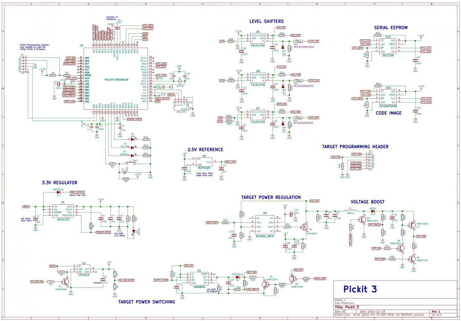
This schematic is very similar to the one Hendrik used, with a couple component changes and a fix for a PNP transistor that was shown backwards on his schematic. I’ll briefly talk about the different sections that I have labeled above. First – in the upper left corner is the pic24 processor that controls this device. It is a PIC24FJ256GB106 mcu. There are the requisite capacitors and 12MHz crystal attached, as well as a programming header to load its firmware. In addition to these components, the USB connector is shown, as well as the status LEDs and OTG Button connections. Directly below the MCU is the MCP1727 voltage regulator. At the bottom is a LTC4411, a MAX893L, and associated circuitry that among a couple other things, controls the power to the programming target, if it is not self-powered, and this device is supplying power to it. Above that is a MCP601 op-amp and voltage boosting circuitry. In the middle of the page is a MCP1525 voltage reference chip and the Target programming header. Top center you will see the three 74LVC1T45 voltage level shifters, and to the right are the 25LC256 EEPROM and also the SST25VF040B serial flash chip used for the Code image when doing OTG programming.
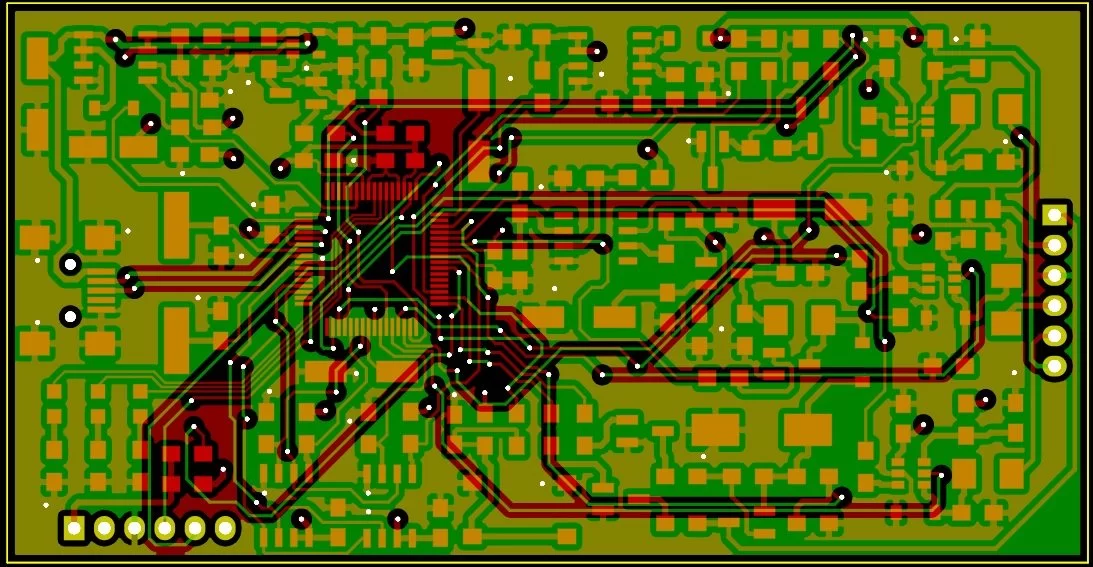
PICKIT 3 CLONE PCB Preview:
After carefully checking my schematic against the one used on the Blog and also against the one published by Microchip – I was satisfied that it was accurate and I moved on to laying out the PCB.
I decided to use a 4 layer board for this design with the following layer stack:
Layer 1 (Top) – Signal and components
Layer 2 – Ground Plane
Layer 3 – Power Planes
Layer 4 – Signal
I decided to use the open-source EDA program Kicad to design a 4 layer SMD project. I had only used it for 2 layer PTH designs previously, but wanted to see how it would do in something a little more complex than the ones I had already done. Here is a link to the completed Kicad project files
Download all PICKIT 3 CLONE Files in KiCad Format:
Download all PICKIT 3 CLONE Files schematic pcb project in KiCad Format
Online tools to view the project:
KiCAD Schematic Viewer
KiCAD PCB Viewer
KiCAD Software Link
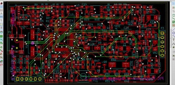
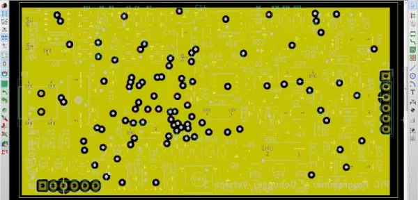
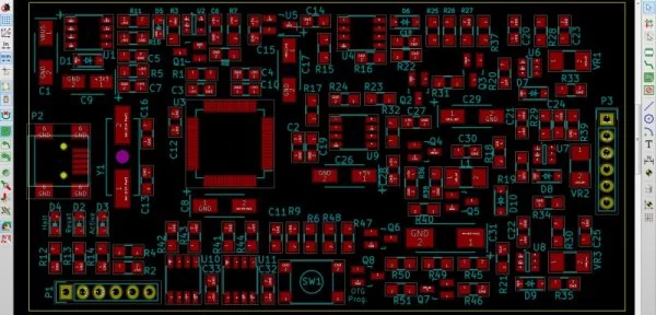
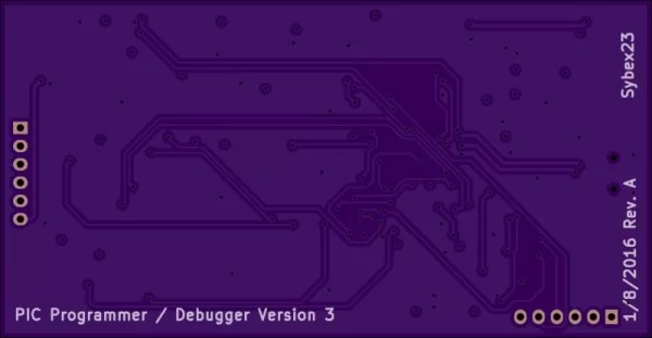
Here are some images of the project in the PCB editor:
The above image shows the front and back signal layers after routing was completed.
Here is an image of the Ground Plane:
An image of the 4 zone power plane I used:
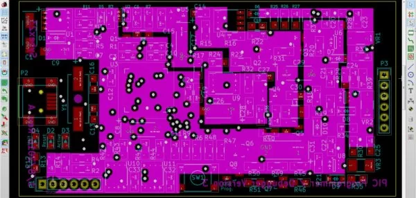
And an image of just the footprint placement:
The 4 zones I used for the power plane were for 3.3V, 5V, and then VDD_INT and VDD_TAR – just to make it a little easier to place components where I wanted without having to route a bunch more traces.
Kicad has a really nice 3d viewer. Here is a rendering of the completed design fully populated with 3d component models:
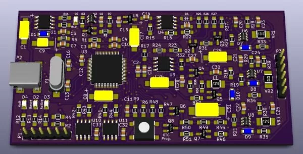
I didn’t have models for a couple of the components like the Inductor or the PTCs that I used, so I just filled them in with resistor models, but you get the idea.
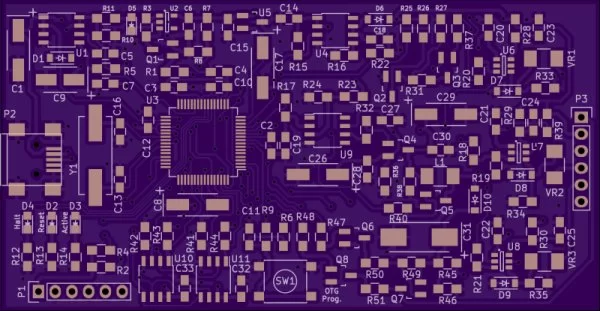
Now that I had everything designed, it was time to send my Gerber files off to get the board made. I uploaded my files over at OSHPark and here are a couple of renderings of what the board would look like based on their interpretation of the Gerbers –
The top of the board:
and the Bottom of the board:
I like using OSHPark because anytime I order boards at OSHPark, the order price includes 3 copies of the design, and also, the boards are really decent quality. I have shared this as an open-source design on their site, so if you are interested in trying this out for yourself and don’t want to have to deal with creating the board, you can just order it from them. Here is the link: Shared Board Files
Now that my board was ordered, I turned my attention to the BOM and getting my parts ordered. Here is an Excel CSV file that contains everything I used – complete with Digikey part numbers. Take notice of the NOTES column where the design has specified Tantalum caps, and also one in particular that needed to have < 1 ohm ESR.
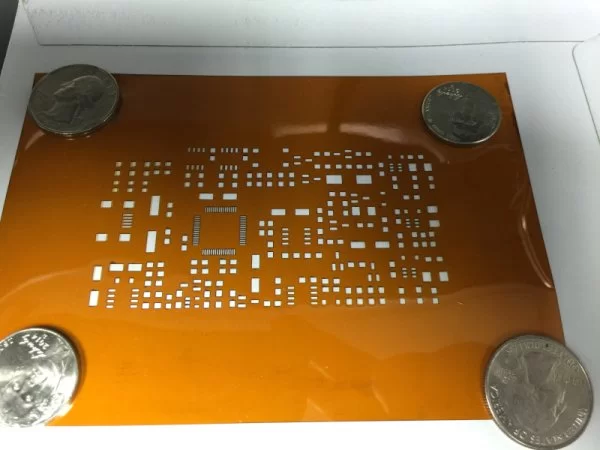
While waiting for my items to arrive, I thought I might try getting a stencil made for this project to make it easier to paste the board prior to component population. So – I ordered one using these files at www.OSHStencil.com. The stencil turned out great – here is what I got:
Fast forward about 2 weeks……
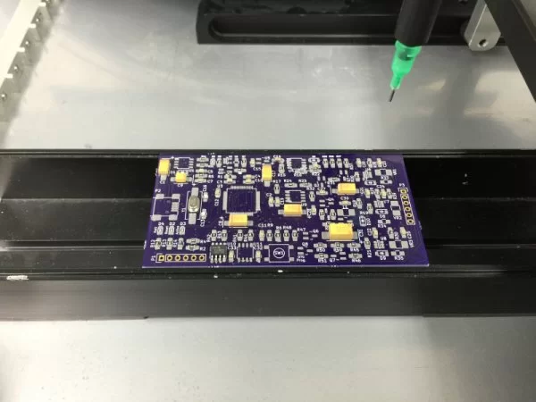
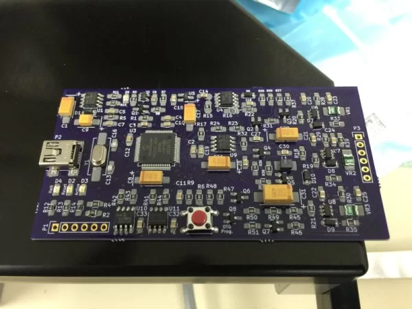
Now that everything had arrived, it was time to build. I used a table-top vacuum device to place the components manually, but a decent set of tweezers and a steady hand would probably work just as well. Here are a couple photos of the board in various stages of completion-
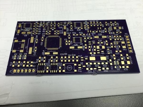
The bare board as received from OSHPark:
The board pasted and components being placed:
The pasted and populated board ready for reflow:
After the board was pasted and populated, it was time to reflow the solder. I was fortunate to have access to a production reflow oven, but any other method should work just fine – toaster oven, hot-plate, skillet, etc… If you are more adventurous than I am, I’m sure you could solder the whole thing by hand. I used 0805 or larger components for everything, and I also used the “Hand-Soldering” footprint variants in Kicad when laying out the PCB, so there is a lot of pad available to solder on if you want to give hand-soldering a go.
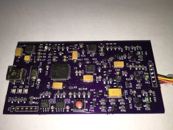
Here is the board after the solder reflow oven completed. Note that I have also soldered on some leads to extend the programming header:
Now for the moment of truth – let’s see if it works:
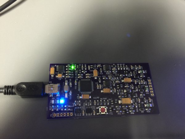
Success!!
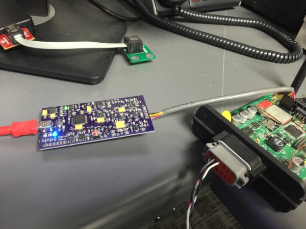
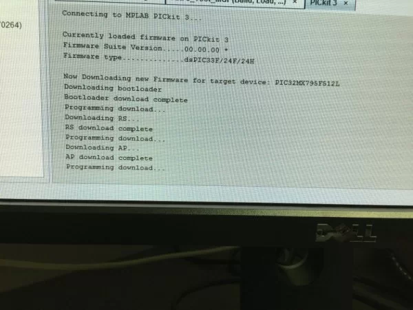
Once it powered up, it was time to load the firmware and see if it would program another board. Here is a photo of my new programmer/debugger programming another device – in this case, a PIC32MX795F512L:
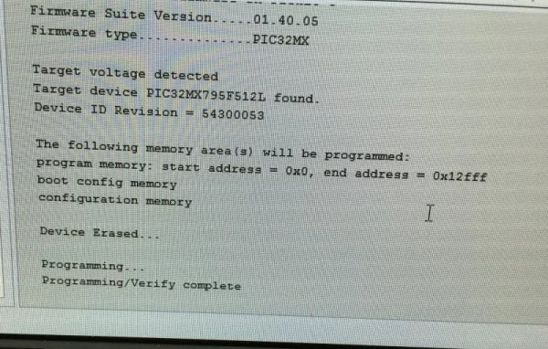
Here is the MPLABX output window loading in the new firmware for this target:
and after a successful programming of the target device:
There you have it – a successful project in every regard. Throughout this post, I have linked everything that I used to complete this project except for the firmware for the Pickit3. Microchip has publicly released the schematics for this device, but I’m not sure what their stance on the firmware is, so I will not host it here. It is easily discovered with a minimum of effort.
Some items of note:
I have tested the ability to program and debug several different pic processors with this device. It works – plain and simple. What I have not yet tested is the OTG programming mode where you can load an image into the serial flash and take it around and program with it that way. I will test that shortly and edit this post to reflect my results.
EDIT – 2/9/2016 – OTG Programming mode worked fine. I was able to load an image and program from the on-board image without any problems. After the test, MPLAB X gave me the option to return to programmer/debugger mode the next time I connected.
Since everything worked so well, I may do a revision of this board and use 0603 or smaller parts, and may place components on the bottom to shrink it down to a smaller size. the current board is 3.58×1.85 inches (90.91×47.09 mm). It’s not all that much larger than an actual Microchip Pickit3, but I’d like to see if I can make it something more along the lines of a USB Thumb Drive sized device.
I am going to see if a colleague of mine will create a CAD file of an enclosure for this device and then 3d print it. If so, I will post pictures and the file(s) here as well.
If you download the files for use in Kicad, you will get an error message that says you are missing component symbols, etc… However, it will still open and work – using the lib-cache file. At some point in the near future, I will create a separate library file with the actual symbols I used and place it in the download directory as well if it is needed, but I think you should be ok to use it as it is.
Read More: MAKING A PICKIT 3 CLONE
About The Author
Ibrar Ayyub
I am an experienced technical writer holding a Master's degree in computer science from BZU Multan, Pakistan University. With a background spanning various industries, particularly in home automation and engineering, I have honed my skills in crafting clear and concise content. Proficient in leveraging infographics and diagrams, I strive to simplify complex concepts for readers. My strength lies in thorough research and presenting information in a structured and logical format.
Follow Us:LinkedinTwitter