
In my previous post, I write about an LED matrix for a marquee. The display itself is a two-board solution, the second board or ‘daughterboard’ piggy-backs on some pin headers from the display board. This second PCB provides the control interface and logic for handling these 64 leds, and passing along control data to any upstream displays.
The controller uses a 595 shift register to provide the ON/OFF control for each of the eight columns. To provide maximum current to these columns, I have used the ULN2803 current-sink driver. The 2803 is basiclly a darlington array which uses a small current to sink up to 500mA, on each channel… and it has 8 channels.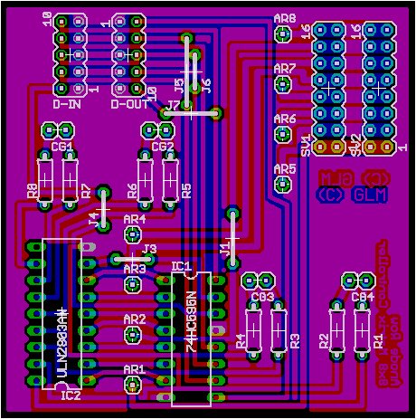 So if I really blast my piranha LEDs with their bleeding edge maximum current of 80mA and the data called for all eight columns to be active at once, the entire column would need a total sink of 640mA! I believe the 595 alone can only sink 200mA. The daughterboard has no circuitry on it for controlling the rows of the matrix – they are just wired in parallel to the daisy chain connectors, which will connect it to a current source on the ‘master control’ or interface board. I plan to use some P-Channel mosfets to handle sourcing potentionally several amps of current. For example, if I connect sixteen of these modules together, and want to turn an entire row on at once, that is 128 LEDs, each drawing 80mA, for a grand total of 10.24A. Wow, that is a lot of power, my goodness, good thing I have a bunch of old AT style switching power supplies laying around, with 15-20A on their 5v rails.
The 595 shift register is just a set of switches, which are set through a synchronous serial interface – a big long string of 1′s and 0′s is clocked out of whatever ends up controlling this marquee (most likely a PIC microcontroller). Each register takes eight bits, thats why I went with eight columns. So if I build a sign with sixteen of these modules, I’ll be pushing 128 bits out a serial port. The entire register will need to be updated for every row, so an entire refresh will take 128 * 8 bits or 1024 bits. At 20mHz, my pic can clock a bit out every two microseconds, so refreshing the entire marquee would take roughly 2.1 milliseconds. A frame rate of 30FPS should be entirely possible, since 1/30th of a second is approximately 33 mS, that leaves a LOT of extra time for the pic to take a nap with… and if I go crazy and build some huge mother of an array, I can beef the pic up to 48mHz, hammering those bits out more than twice as fast.
The display modules are ‘modular’. Daisy-chain connectors provide pass-through of the row current, and data-control signals from the microcontroller. The D-IN port connects the ‘upstream’ registers serial output (QH*) to the current registers serial input (SER), the D-OUT port connects this registers serial output to the next registers input. The rest of the signals are straight parallel. Only changes in the software of the microcontroller would be required to add or subtract display modules from the finished array.
The pcb design and layout is ‘diy compatible’ I’ve used all through-hole components, and jumpers instead of via’s. If I send these out to be fabbed, I’ll probably change the signal routing around, switching the jumpers to vias, perhaps I’ll go with smt ICs, depends on how the layout works out… I might keep the through-hole because I like being able to run signals between the pins and under the ICs, which is hard to do when they’re tiny!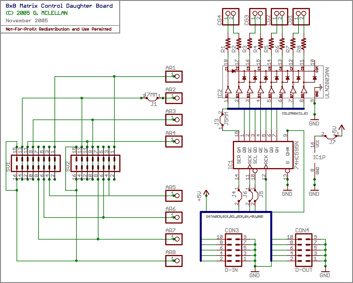 The notations “dont move” are just to remind myself (or anyone else) that you can’t move the ARx (anode row) and CGx (column group) connectors, because they’re specificly positioned to mate with the display board.
composite image of controller layout and top+bottom layers.
same disclaimer as my earlier post, these designs and images are not public domain… please read the disclaimer in my earlier post.
For more detail: Iron in the Fire II
