Summary of High Power High Efficiency Buck Converter Circuit using TL494
A high-efficiency buck (step-down) converter using the TL494 PWM controller is designed, explained, and tested. The article covers buck operation (transistor on/off, inductor and capacitor roles), TL494 internals (reference, oscillator, dead-time control, error amplifiers, output control, output transistors), component list, schematic, and construction notes including PCB reinforcement for high current and use of jumpers to prevent trace burnout.
Parts used in the High-Efficiency Buck Converter:
- TL494 IC - 1
- TIP2955 Transistor - 1
- Screw Terminal 5mmx2 - 2
- 1000uF 60V Capacitor - 1
- 470uF 60V Capacitor - 1
- 50K 1% Resistor - 1
- 560R Resistor - 1
- 10K 1% Resistor - 4
- 3.3K 1% Resistor - 2
- 330R Resistor - 1
- 0.22uF Capacitor - 1
- 5.6K 1W Resistor - 1
- 12.1V Zener Diode - 1
- MBR20100CT Schottky Diode - 1
- 70uH Inductor (27 x 11 x 14 mm) - 1
- Potentiometer 10K Trim-Pot - 1
- 0.22R Current Sense Resistor - 2
- Clad Board Generic 50x50mm - 1
- PSU Heat Sink Generic - 1
- Jumper Wires Generic - 15
A buck converter (step-down converter) is a DC-to-DC switching converter that steps down voltage while maintaining a constant power balance. The main feature of a buck converter is efficiency, which means with a buck converter on board, we can expect extended battery life, reduced heat, smaller size, and improved efficiency. We previously made a few simple Buck converter circuits and explained its basics and design efficiency.
So, in this article, we are going to design, calculate and test a high-efficiency buck converter circuit based on the popular TL494 IC and at last, there will be a detailed video showing the working & testing part of the circuit, So without further ado, let’s get started.
How does a Buck Converter work?
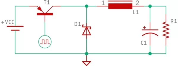
The above figure shows a very basic buck converter circuit. To know how a buck converter works, I am going to divide the circuit into two conditions. The first condition when the transistor is ON, next condition when the transistor OFF.
Transistor On state
In this scenario, we can see that the diode is in open circuit condition because it’s in the reverse-biased state. In this situation, some initial current will start flow through the load, but the current is restricted by the inductor, thus the inductor also starts to charge up gradually. Therefore, during the on-time of the circuit, the capacitor builds up the charge cycle by cycle, and this voltage reflects across the load.
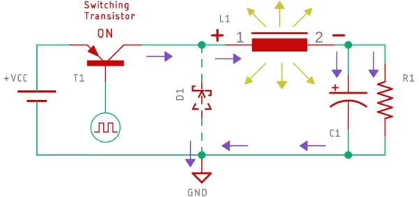
Transistor Off state
When the transistor is in an off state, the energy stored in the inductor L1 collapses and flows back through the diode D1 as shown in the circuit with the arrows. In this situation, the voltage across the inductor is in reverse polarity and so the diode is in forward-bias condition. Now due to the collapsing magnetic field of the inductor, the current continues to flow through the load until the inductor runs out of charge. All this happens while the transistor is in off condition.
After a certain period when the inductor is almost out of stored energy, the load voltage starts to fall again, in this situation, the capacitor C1 becomes the main source of current, the capacitor is there to keep the current flowing until the next cycle begins again.
Now by varying the switching frequency and switching time, we can get any output from the 0 to Vin from a buck converter.
IC TL494
Now before going to build a TL494 buck converter, let’s learn how the PWM controller TL494 works.
The TL494 IC has 8 functional blocks, which are shown and described below.
The 5V internal reference regulator output is the REF pin, which is pin-14 of the IC. The reference regulator is there to provide a stable supply for internal circuitry like the pulse-steering flip-flop, oscillator, dead-time control comparator, and PWM comparator. The regulator is also used to drive the error amplifiers which are responsible for controlling the output.
Note! The reference is internally programmed to an initial accuracy of ±5% and maintains stability over an input voltage range of 7V to 40 V. For input voltages less than 7V, the regulator saturates within 1V of the input and tracks it.
2. Oscillator
The oscillator generates and provides a sawtooth wave to the dead time controller and the PWM comparators for various control signals.
The frequency of the oscillator can be set by selecting timing components RT and CT.
The frequency of the oscillator can be calculated by the formula below
Fosc = 1/(RT * CT )
For simplicity, I have made a spreadsheet, by which you can calculate the frequency very easily.
Note! The oscillator frequency is equal to the output frequency only for single-ended applications. For push-pull applications, the output frequency is one-half of the oscillator frequency.
3. Dead-time Control Comparator
The dead time or to simply say off-time control provides the minimum dead time or off-time. The output of the dead time comparator blocks switching transistors when the voltage at the input is greater than the ramp voltage of the oscillator. Applying a voltage to the DTC pin can impose additional dead time, thus providing additional dead time from its minimum of 3% to 100% as the input voltage varies from 0 to 3V. In simple terms, we can change the Duty cycle of the output wave without tweaking the error amplifiers.
Note! An internal offset of 110 mV ensures a minimum dead time of 3% with the dead-time control input grounded.
4. Error Amplifiers
Both high-gain error amplifiers receive their bias from the VI supply rail. This permits a common-mode input voltage range from –0.3 V to 2 V less than VI. Both amplifiers behave characteristically of a single-ended single-supply amplifier, in that each output is active high only.
5. Output-Control Input
The output-control input determines whether the output transistors operate in parallel or push-pull mode. By connecting the output control pin which is pin-13 to ground sets the output transistors in parallel operation mode. But by connecting this pin to the 5V-REF pin sets the output transistors in push-pull mode.
6. Output Transistors
The IC has two internal output transistors which are in open-collector and open-emitter configurations, by which it can source or sink a maximum current up to 200mA.
Note! The transistors have a saturation voltage of less than 1.3 V in the common-emitter configuration and less than 2.5 V in the emitter-follower configuration.
Features of TL494 IC
- Complete PWM Power-Control Circuitry
- Uncommitted Outputs for 200-mA Sink or Source Current
- Output Control Selects Single-Ended or Push-Pull Operation
- Internal Circuitry Prohibits Double Pulse at Either Output
- Variable Dead Time Provides Control Over Total Range
- Internal Regulator Provides a Stable 5-V
- Reference Supply With 5% Tolerance
- Circuit Architecture Allows Easy Synchronization
Note! Most of the internal schematic and operations description is taken from the datasheet and modified to some extent for better understanding.
Components Required
- TL494 IC – 1
- TIP2955 Transistor – 1
- Screw Terminal 5mmx2 – 2
- 1000uF,60V Capacitor – 1
- 470uF,60V Capacitor – 1
- 50K,1% Resistor – 1
- 560R Resistor – 1
- 10K,1% Resistor – 4
- 3.3K,1% Resistor – 2
- 330R Resistor – 1
- 0.22uF Capacitor – 1
- 5.6K,1W Resistor – 1
- 12.1V Zener Diode – 1
- MBR20100CT Schottky Diode – 1
- 70uH (27 x 11 x 14 ) mm Inductor – 1
- Potentiometer (10K) Trim-Pot – 1
- 0.22R Current Sense Resistor – 2
- Clad Board Generic 50x 50mm – 1
- PSU Heat Sink Generic – 1
- Jumper Wires Generic – 15
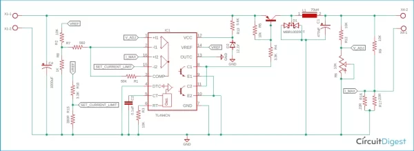
Schematic Diagram
Circuit diagram for High-Efficiency Buck Converter is given below.
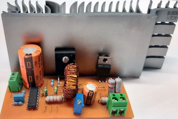
Circuit Construction
For this demonstration of this high current buck converter, the circuit is constructed in handmade PCB, with the help of the schematic and PCB design files [Gerber file]; please note that if you are connecting a big load to the output buck converter then a huge amount of current will flow through the PCB traces, and there’s a chance that the traces will burn out. So, to prevent the PCB traces from burning out I have included some jumpers which help to increase the current flow. Also, I have reinforced the PCB traces with a thick layer of solder to lower the trace resistance.
Source: High Power High Efficiency Buck Converter Circuit using TL494
- How does a buck converter step down voltage?
By switching a transistor on and off so the inductor stores energy during on-time and releases it through the diode and capacitor during off-time, smoothing the output to a lower voltage. - Can the TL494 provide a stable reference for the circuit?
Yes, the TL494 provides an internal 5V reference regulator (pin 14) with initial accuracy of ±5% for internal circuitry and error amplifiers. - What determines the oscillator frequency in the TL494?
The oscillator frequency is set by timing components RT and CT and is calculated by Fosc = 1/(RT * CT). - How is dead time controlled in the TL494?
The dead-time control comparator uses the DTC pin; applying 0 to 3V imposes additional dead time from a minimum of about 3% to 100%. - Does the TL494 support single-ended and push-pull outputs?
Yes, the output-control input (pin 13) selects parallel (single-ended) when grounded or push-pull when tied to the 5V REF pin. - What precautions are recommended when building the PCB for high current?
Include jumpers to increase current capacity, reinforce PCB traces with a thick solder layer, and use proper heat sinking to prevent trace burnout. - What is the role of the capacitor when the transistor is off?
The capacitor supplies current to the load while the inductor's stored energy depletes, maintaining output until the next switching cycle. - What are the output transistor capabilities in the TL494?
The IC has two open-collector/open-emitter transistors that can source or sink up to 200mA with specified saturation voltages.