Summary of dsPIC33 Active Power Factor Correction using dsPIC33FJ12MC202 with Proteus Simulation
This project implements Active Power Factor Correction (PFC) using a dsPIC33FJ12MC202 microcontroller, following Microchip AN1106. It uses synchronized ADC sampling and high-frequency PWM to run voltage and current PI control loops (inside an ADC interrupt), driving a PFC MOSFET stage in Proteus VSM simulation. The design regulates a DC bus while shaping input current to follow AC voltage, and includes power-on delay, fault handling, and simulation validation suitable for embedded power electronics study and hardware porting.
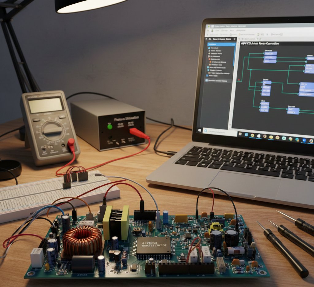
Parts used in the dsPIC33 Active Power Factor Correction Project:
- dsPIC33FJ12MC202 microcontroller
- Bridge rectifier
- PFC inductor
- Power MOSFETs
- DC bus capacitors
- Voltage sensing network
- Current sensing network
- PWM gate driver stage
- AC voltage source (simulation)
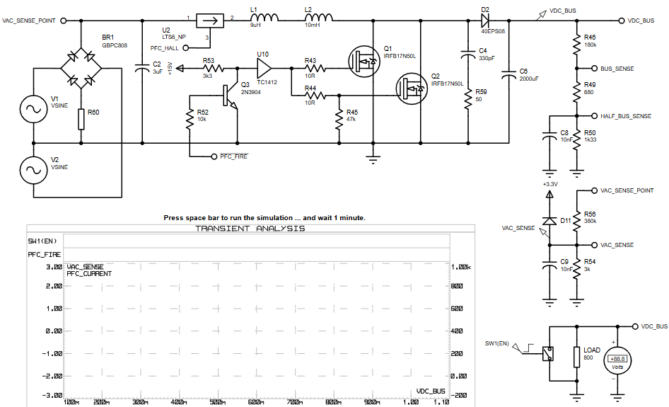
- Why is Proteus simulation used for this project?
Proteus allows safe testing of high-voltage PFC control without real hardware risks. - Can this code run on other dsPIC33 devices?
It is optimized for dsPIC33FJ12MC202 but can be ported with peripheral changes. - Why is ADC triggered by PWM?
To ensure sampling occurs at consistent points in the switching cycle. - What causes unstable DC bus voltage in simulation?
Incorrect PI parameters, ADC scaling errors, or PWM frequency mismatch. - Can this project be extended to hardware?
Yes, it is based on a Microchip reference design intended for real systems. - Why is there a power-on delay?
To allow DC bus capacitors to charge safely before enabling PFC switching. - What PWM frequency is used?
The firmware configures PWM for high-frequency operation suitable for PFC. - Is this suitable for beginners?
Best suited for intermediate users familiar with embedded power control.