Summary of Blink Led with Pic18f2550,PIC18F2455,PIC18F4455,Pic18F4550 Microcontroller….20Mhz Crystal frequency…
This article guides beginners through a PIC18F2550 LED blinker project as a precursor to USB development. It details the challenges of configuring microcontroller bits, comparing MPLAB IDE and MPLABX IDE workflows. The author explains how to set up an external 20 MHz crystal, manipulate Port-A pins using C code, and highlights differences in hex file generation and delay function execution between the two environments.
Parts used in the PIC18F2550 LED Blinker:
- PIC18F2550 Microcontroller
- LED (Light Emitting Diode)
- External 20 MHz Crystal Oscillator
- MPLAB IDE Software
- MPLABX IDE Software
- C18 Compiler
- High Tec C Compiler
Pic microcontroller code Mplab ide
In simple MPLAB IDE I am manually setting the configuration bits in the configuration window and after compiling the code with c18 compiler i am exporting the hex file containing the configuration bit code. Note that the output compiled code hex file in MPLAB ide does not contains the config info. For proper config bits hex file, you have to import it from the file>Import-Hex.
The code in MPLABX contains the fuses bits included in it so the hex file generated in this case contains the config bit info in it. We don’t need to export file from any other window feature.
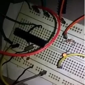
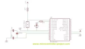
Pic18 microcontroller blink led – Project circuit
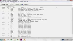
Configuration bits settings for pic microcontroller in mplab ide
You have to set PLLDIV, CPUDIV and USBPLL configuration bits correctly which matches to the crystal frequency you are using. Configuration settings are given below.
Pic18 microcontroller mplab ide code
TRISAbits.XXX command is used to initialize the individual pins of pic microcontroller in mplab ide as input or output. PORTAbits.XXX command is used to write to individual microcontroller pins in mplab ide. We can directly initialize the whole port by accessing the whole TRISA register simply by TRISA=input/output. Same as we can write to whole port at once by PORTA=high/low.
#include<stdio.h>
#include”p18f2550.h”
#define _XTAL_FREQ 20e6
void delay();
void delay(){
unsigned int i=0,j=0;
for(i=0;i< 20;i++)
for(j=0;j< 5000;j++);
}
void main()
{
/*TRISAbits.RA0=0; //Port-B as Output
TRISAbits.RA1=0; //Port-B as Output
TRISAbits.RA2=0; //Port-B as Output
TRISAbits.RA3=0; //Port-B as Output
TRISAbits.RA4=0; //Port-B as Output*/
TRISA=0b00000000;
while(1){
/*PORTAbits.RA0=1;
PORTAbits.RA1=1;
PORTAbits.RA2=1;
PORTAbits.RA3=1;
PORTAbits.RA4=1;*/
PORTA=0xFF;
//PORTA=0x00;
delay();
/*PORTAbits.RA0=0;
PORTAbits.RA1=0;
PORTAbits.RA2=0;
PORTAbits.RA3=0;
PORTAbits.RA4=0;*/
PORTA=0x00;
delay();
//PORTA=0xFF;
}
}
Pic microcontroller code in mplabx ide
/*
* File: blinky.c
* Author: Usman Ali Butt
* Property: microcontroller-project.com
* Created on 28 May, 2016, 12:17 PM
*/
//#include <stdio.h>
//#include <stdlib.h>
#include <p18f2550.h>
#define _XTAL_FREQ 20000000
void delay();
// CONFIG1L
#pragma config PLLDIV = 5 // PLL Prescaler Selection bits (Divide by 5 (20 MHz oscillator input))
#pragma config CPUDIV = OSC1_PLL2// System Clock Postscaler Selection bits ([Primary Oscillator Src: /1][96 MHz PLL Src: /2])
#pragma config USBDIV = 2 // USB Clock Selection bit (used in Full-Speed USB mode only; UCFG:FSEN = 1) (USB clock source comes from the 96 MHz PLL divided by 2)
// CONFIG1H
#pragma config FOSC = HS // Oscillator Selection bits (HS oscillator (HS))
#pragma config FCMEN = OFF // Fail-Safe Clock Monitor Enable bit (Fail-Safe Clock Monitor disabled)
#pragma config IESO = OFF // Internal/External Oscillator Switchover bit (Oscillator Switchover mode disabled)
// CONFIG2L
#pragma config PWRT = OFF // Power-up Timer Enable bit (PWRT disabled)
#pragma config BOR = ON // Brown-out Reset Enable bits (Brown-out Reset enabled in hardware only (SBOREN is disabled))
#pragma config BORV = 3 // Brown-out Reset Voltage bits (Minimum setting 2.05V)
#pragma config VREGEN = OFF // USB Voltage Regulator Enable bit (USB voltage regulator disabled)
// CONFIG2H
#pragma config WDT = OFF // Watchdog Timer Enable bit (WDT disabled (control is placed on the SWDTEN bit))
#pragma config WDTPS = 32768 // Watchdog Timer Postscale Select bits (1:32768)
// CONFIG3H
#pragma config CCP2MX = ON // CCP2 MUX bit (CCP2 input/output is multiplexed with RC1)
#pragma config PBADEN = OFF // PORTB A/D Enable bit (PORTB<4:0> pins are configured as digital I/O on Reset)
#pragma config LPT1OSC = OFF // Low-Power Timer 1 Oscillator Enable bit (Timer1 configured for higher power operation)
#pragma config MCLRE = ON // MCLR Pin Enable bit (MCLR pin enabled; RE3 input pin disabled)
// CONFIG4L
#pragma config STVREN = OFF // Stack Full/Underflow Reset Enable bit (Stack full/underflow will not cause Reset)
#pragma config LVP = OFF // Single-Supply ICSP Enable bit (Single-Supply ICSP disabled)
#pragma config XINST = OFF // Extended Instruction Set Enable bit (Instruction set extension and Indexed Addressing mode disabled (Legacy mode))
// CONFIG5L
#pragma config CP0 = OFF // Code Protection bit (Block 0 (000800-001FFFh) is not code-protected)
#pragma config CP1 = OFF // Code Protection bit (Block 1 (002000-003FFFh) is not code-protected)
#pragma config CP2 = OFF // Code Protection bit (Block 2 (004000-005FFFh) is not code-protected)
#pragma config CP3 = OFF // Code Protection bit (Block 3 (006000-007FFFh) is not code-protected)
// CONFIG5H
#pragma config CPB = OFF // Boot Block Code Protection bit (Boot block (000000-0007FFh) is not code-protected)
#pragma config CPD = OFF // Data EEPROM Code Protection bit (Data EEPROM is not code-protected)
// CONFIG6L
#pragma config WRT0 = OFF // Write Protection bit (Block 0 (000800-001FFFh) is not write-protected)
#pragma config WRT1 = OFF // Write Protection bit (Block 1 (002000-003FFFh) is not write-protected)
#pragma config WRT2 = OFF // Write Protection bit (Block 2 (004000-005FFFh) is not write-protected)
#pragma config WRT3 = OFF // Write Protection bit (Block 3 (006000-007FFFh) is not write-protected)
// CONFIG6H
#pragma config WRTC = OFF // Configuration Register Write Protection bit (Configuration registers (300000-3000FFh) are not write-protected)
#pragma config WRTB = OFF // Boot Block Write Protection bit (Boot block (000000-0007FFh) is not write-protected)
#pragma config WRTD = OFF // Data EEPROM Write Protection bit (Data EEPROM is not write-protected)
// CONFIG7L
#pragma config EBTR0 = OFF // Table Read Protection bit (Block 0 (000800-001FFFh) is not protected from table reads executed in other blocks)
#pragma config EBTR1 = OFF // Table Read Protection bit (Block 1 (002000-003FFFh) is not protected from table reads executed in other blocks)
#pragma config EBTR2 = OFF // Table Read Protection bit (Block 2 (004000-005FFFh) is not protected from table reads executed in other blocks)
#pragma config EBTR3 = OFF // Table Read Protection bit (Block 3 (006000-007FFFh) is not protected from table reads executed in other blocks)
// CONFIG7H
#pragma config EBTRB = OFF // Boot Block Table Read Protection bit (Boot block (000000-0007FFh) is not protected from table reads executed in other blocks)
/*
*
*/
void main(void) {
TRISA=0x00; //Pic microcontroller Port-A as OUTPUT
while(1){
PORTA=0x00;
delay();
PORTA=0xFF;
delay();
}
}
void delay(){
int i=0,j=0;
for (i=0;i<=5000;i++)
for(j=0;j<=5;j++);
}
I tested both codes with pic micrococntroller. Both works fine. The only difference is in delay function. Mplab code delay is larger than the mplabx ide delay. I intentionally made difference to check if both the codes delay functions are working fine with the same 20 Mhz crystal.
Source: Blink Led with Pic18f2550,PIC18F2455,PIC18F4455,Pic18F4550 Microcontroller….20Mhz Crystal frequency…
- Why is setting configuration bits difficult?
It requires careful study of the datasheet to match settings like PLLDIV and CPUDIV with the specific crystal frequency used. - Can I use a different crystal frequency than 20 MHz?
No, if you do not use a 20 MHz crystal, the microcontroller circuit will not work unless you adjust the configuration bits for your specific crystal. - How does the hex file differ between MPLAB IDE and MPLABX IDE?
MPLAB IDE generates a hex file without config info requiring manual import, while MPLABX includes fuse bits directly in the generated hex file. - What commands initialize pins as input or output in MPLAB IDE?
The TRISAbits.XXX command initializes individual pins, while accessing the whole TRISA register initializes the entire port at once. - How do I write data to the microcontroller pins?
You can use PORTAbits.XXX for individual pins or assign values like high/low directly to the PORTA register for the whole port. - Are the header files identical in both IDEs?
The header files are essentially the same, though there is a slight syntax difference where one uses double quotes and the other uses parentheses. - Which compiler is used for the code examples?
The code is written using the C18 compiler in MPLAB IDE and the High Tec C compiler in MPLABX IDE. - Does the delay function behave differently in each IDE?
Yes, the delay function in the MPLAB code is larger than the one in the MPLABX code, even though both run on the same 20 MHz crystal.