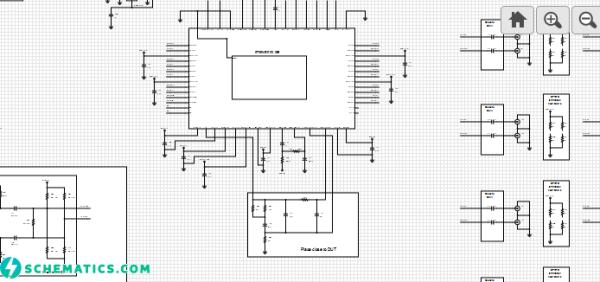
This reference design features the 8T49NS010 integrated circuit that functions as a clock synthesizer with a built-in fanout buffer and divider. By using an external clock source or a crystal, the 8T49NS010 can generate high performance timing geared towards the communications and datacom markets, especially for applications demanding extremely low phase noise jitter, such as 10, 40 and 100GE. Depending on the input used, the 8T49NS010’s low phase noise integer-N PLL can multiply the reference to 2400MHz or 2500MHz.
The device offers ten clock outputs (QCLK[9:0]/nQCLK[9:0]). Each output can be disabled individually through registers. With ÷2, ÷4, ÷8 and ÷16 values one can get output frequencies of 156.25MHz, 312.5MHz, 625MHz and 1250MHz when driven from a 25MHz input, for example. The input select pin REF_SEL will choose either XTAL input or CLK_IN input will be used and this pin also set the pre-divider PRE to either x2 or ÷1. The feedback divider FB_SEL pin will set the feedback divider to either ÷50, ÷25. The feedback divider should be properly set to assure the PLL lock for VCO=2.5GHz. The N1 and N0 are pins for output frequency divider setting. Aside from the divider values that can be set using pins N1 and N0, additional divider values are available through registers that can be programmed with I2C interface. This reference design recommends the FT2232 USB to UART converter to program the device divider value via I2C pins. The 8T49NS010 operates over the industrial temperature range of -40°C to +85°C with a 3.3V supply voltage.
The 8T49NS010 provides versatile frequency configurations and output format that is optimized to deliver excellent phase noise performance.
For more detail: 8T49NS010 Clock Synthesizer and Fanout Buffer/Divider
