Another look at the hardware in the SDS7102
I’ve been a bit busy with work lately and haven’t had time to do a lot of hacking on the scope. This is a write-up of stuff I did quite some time ago so I hope I haven’t forgotten anything important.
Except for soldering some wires to the JTAG and serial port on the scope, most of the discoveries about the SDS7102 I have made so far has been done with just software and a bit of thinking. But I was running out of things I could find out this way.
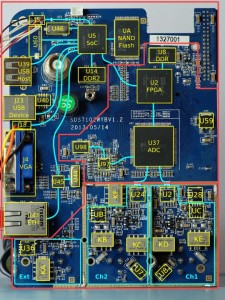
To be able to find out more it was time to crack the scope open again and take another look at the hardware. I also desoldered the shield covering the analog frontend (AFE) so that I could see what was hidden behind it. Here are two photos of the front and back of the main circuit board (click on the images for lager versions).
Lets take a look at the functional blocks of the main board, and see what I have discovered so far and see what works with Linux.
An Embedded Computer
The first functional block of the scope is a rather generic embedded computer based around a Samsung 2416 System on Chip (SoC). The SoC contains a 400MHz ARM9 processor with a lot of built in peripherals such as display controller, USB host and device controllers, serial ports (UART), a JTAG interface for debugging and a few more peripherals that aren’t used in this design. This SoC together with a DDR2 memory and a NAND flash comprises a complete little embedded computer. The SDS7102 designers have also tacked on an external 10/100Mbit ethernet controller and external VGA controller.
Lets start with the components on the back of the main board.
U5 is the Samsung S3C2416 SoC. It’s mostly supported by Linux.
J5 is a connector with JTAG pins from the SoC.
U46 is the main 12MHz crystal for the SoC
UA a 128MBbyte K9F1G08U0D Samsung NAND flash. It’s connected to the the external bus controller on the SoC. It seems to work fine with the S3C2412 NAND flash driver built into the Linux kernel.
U14 is a 64MByte Hynix “H5PS5162GFR 512Mbit DDR2 SDRAM” memory. It’s connected to the SDRAM controller of the SoC. It’s initialized by the bootloader and works fine in Linux.
U60 is a mystery connector which has not been populated. A lot of wires head off in the direction of the SoC. I’m a bit curious about what it does.
U39 is the low/full speed USB host connector. It’s connected to the USB host controller on the SoC and works fine with the OHCI driver in Linux.
U40 is a TI TPS2041 “Power distribution switch” which I believe provides power to the USB host port. This switch has an enable input and an over-current output. Both could have been connected to the SoC to allow control and monitoring of the USB host port voltage but as far as I can tell the enable input is hardwired to always on and there’s nothing that monitors the output. So all this chip seems to do is to provide over-current protection for the USB port.
J23 is the low/full/high speed USB device connector. It’s connected to the USB device controller on the SoC and works fine with the S3C_HSUDC USB device driver in Linux. GPF2 on the SoC is used to detect the presence of VBUS on the connector.
J18 is a pin header that’s not populated. It is connected to the first serial port (UART0) on the SoC and uses 3.3V signaling. It works fine with the S3C_UART driver in Linux.
UJ4 is the VGA connector. More about that later.
U45 is a KSZ8851SNL 10/100Mbit ethernet controller (Note that it’s the SNL version of the chip with a SPI interface). It is connected to the high speed SPI (HSSPI) port on the SoC. It works fine with the KS8851 driver in Linux.
U44 is a 25MHz crystal for the ethernet controller.
U43 is the Ethernet connector.
There’s also a buzzer next to the BNC connector. I have never heard it make noise, despite changing most of the GPIO ports configured as outputs on the SoC. I wonder how it is connected.
Let’s take a look at the front of the main board.
I’ve added a box showing the position of the SoC (U5) on the other side of the board.
JA is the LCD board connector. The pins are connected to the LCD controller of the SoC. One more pin, GPB3, is used to control the brightness of the display. It works fine with the S3C_FB driver Linux.
U63 is a Chrontel CH7206 “TV/VGA Encoder” which translates the LCD display signals into a VGA signal. I’ve already discovered that the I2C bus used to control this chip is connected to GPB4 and GPB9 on the SoC and I can talk to it using the i2c-gpio driver in Linux. I haven’t tried configuring the VGA controller yet it shouldn’t be that hard to make it work.
J4 is the VGA connector which is wired up to the VGA controller.
U9, a 74AC08 “Quad AND Gate” seems to be a driver for some of the signals from the VGA controller. Everything is hardwired so there’s nothing to configure here.
UF is a footprint for a component that is not populated. It seems to be connected to the serial port. My guess is that it would be possible to add a RS232 driver here so the serial port will use RS232 levels instead of 3.3V, but I’m not sure.
U58 is a mystery component, I can’t even decipher the markings on it. It seems to be connected to a large inductor (L1) next to it, so my guess is that it is some kind of power supply and hopefully it won’t need any configuration.
U12 is the connector for the front panel with all the buttons and rotary switches on the scope. I haven’t even started looking at how it is wired up.
As I said, all of this makes up a small embedded ARM computer and except for the VGA controller and the front panel everything works just fine with Linux. I had to add some ugly hacks to the USB device driver, but it really wasn’t that hard to get everything to work.
Signal Processing
The second functional block consists of an Analog to Digital Converter (ADC) which converts the signals from the analog frontend to digital signals which are then processed by the FPGA. There is also a DDR memory connected to the FPGA which is used to store the traces. The FPGA is connected to the SoC via two buses, one bus is used to configure the FPGA the other bus is used by the SoC to retrieve traces from the FPGA and show them on the screen.
U2 is the FPGA, a Xilinx Spartan 6 SC6SLX9. I have figured out how to configure the FPGA using the Xilinx Slave Serial mode. GPK3, GPK5, GPK7, GPK11 and GPK13 on the Soc are connected to CCLK, DONE, PROG_B, DIN and INIT_B on the FPGA.
The FPGA is connected to the SoC via some kind of high bandwidth bus, probably via the resistor banks to the left of the FPGA. I’m hoping that the FPGA is connected the same bus as the NAND flash, but I have a sneaking suspicion that it isn’t.
U8 is a DDR2 memory, the same Hynix 64MByte model that is used for the SoC’s memory. I need to figure out how it is connected to the FPGA. The FPGA has a built in hard SDRAM controller which supports DDR2 memory, so hopefully they have used one of the default Xilinx Memory Interface Generator (MIG) pinout. If not, this can be a bit tricky to say the least since all of the pins are hidden under the BGA packages and can not be probed.
U37 is the ADC, a Texas Instruments ADC08D500 which can sample two channels at 500Msamples/second with 8 bits of resolution. It can also combine the two channels into one channel which can be sampled at 1Gsamples/second. The footprint on the PCB is a bit strange, apparently it’s prepared for a chinese clone of the ADC08D500 called MXT2000 which has a few extra unused pins but which is otherwise compatible.
The ADC uses a SPI bus for control and I need to figure out where its CS/CLK/DIN pins are connected. It’s possible to see a lot of differential traces going from the ADC to the FPGA. These are probably the sampling clock and digital data. I need to figure out how the they are connected to the FPGA. That ought to be fairly easy as soon as I have managed to talk to the ADC over SPI and set up a known configuration. There might also be some other pins that are interesting such as the RST or CAL inputs or the over-range output.y
U97 is an ADF4360-7 “Integrated Synthesizer and VCO”. It can generate clock frequencies between 350MHz and 1800MHz from a reference clock. The output clock is then used by the ADC as the sampling clock. It uses a SPI bus for control. I need to figure out where its CS/CLK/DIN pins are connected. And maybe a few more pins such as the MUXOUT.
U98 is a a 10MHz crystal oscillator (XO) which provides a very stable reference frequency for the clock synthesizer.
U59 is a voltage regulator. I’m not sure if it’s used by the FPGA or by something else, but there is nothing that should be software controlled so it doesn’t matter that much.
There aren’t that many components related to signal processing on the back.
U52 is a TI TPS65051 “Automotive 6-channel Power Management IC (PMIC)”. It probably provides most of the power rails needed by the FPGA. As with the USB power switch it has a couple of enable inputs that could have been software controlled but I don’t think they are; it looks like they are hardwired to be always on.
U38 is an Atmel AT88SC0104CRF “CryptoMemory”, basically an I2C memory with encryption. It doesn’t have anything to do with signal processing but it sits next to the FPGA. It probably stores the serial number in an encrypted format which is used for some kind of copy protection. I have not figured out how to talk to this chip yet, and even if I do, the contents are encrypted which means I won’t be able to do anything with the information.
There are a few more resistor packs to the right of the FPGA which are probably used for the bus to the the SoC.
The external trigger output and the probe compensation outputs are probably driven by the FPGA, but I don’t know how yet.
Even though there aren’t that many components there are lots of things to discover here. The DDR memory bus and the bus to the SoC are my two big worries.
Analog Frontend
The third functional block is the the Analog Frontend (AFE). The AFE takes the input signals from the scope probes, attenuates or amplifies the signals so that they will have a suitable voltage to be fed to the ADC. This section also performs triggering on the analog signals from the channel inputs and the external trigger inputs.
Analog electronics aren’t my strongest point so I can’t really explain how all this works. “tinhead” traced out the signals of the frontend on his SDS7102 scope and drew a schematic which you can find on the EEVblog forums. I’m mostly interested in the components that have digital connections which can be controlled by software in the SoC or the FPGA. Unfortunately it seems that tinhead’s scope and my scope have slightly different frontends. I hope the differences won’t be too big.
The two input channels Ch1 and Ch2 are almost identical.
U7 and U8 are solid state relays which are used to select AC or DC coupling for Ch2 and Ch1. If the relay is inactive the signal from the probe input will pass through the capacitor next to it and the signal will be AC coupled. If the relay is active it shorts out the capacitor and the input will become DC coupled. This relay probably needs some kind of drive circuit which is then connected to an I/O pin on the SoC or the FPGA. Since some the relays click when I toggle GPIO pins on the SoC I would also guess that the solid state relays are controlled from the SoC.
KB, KC, KD and KE are mechanical relays that select the input attenuation for Ch2 and Ch1. They definitely need some kind of drive circuit, the outputs from the SoC are going to be much too weak to drive a relay. When I was writing data to random GPIO pins on the SoC earlier I could hear relays switching so I know that the relays are controlled by the SoC.
UB and UC are two Analog Devices ADA4817-1 “Single, Low Noise, 1 GHz FastFET” operational amplifiers (OP Amps), one for each channel. I don’t know exactly what they do. As far as I can tell there are no digital signals to control on them.
U24 and U2 are TI LMH6518 “900 MHz, Digitally Controlled, Variable Gain Amplifiers”, one per channel. They are configured via a SPI bus. I need to figure out where these pins, chip select/latch enable, clock and data in are connected.
Next to the external trigger input there is more OP Amp, U36 and one more mechanical relay KA. I don’t know exactly what they do. First I want to figure out how the relay is controlled and later I can try to figure out how it works.
There is yet one more mechanical relay KF. Since there is only one relay and two channels I don’t think it has anything to do with Ch2 which is where it’s physically located. I first need to figure out how to control it and later figure out what it does.
U28 near Ch1 seems to be a voltage regulator. There are no digital controls I hope.
There are a lot of passive components and a few transistors for each channel. It would be possible to trace out how all the components are connected but I’m probably not going to do it.
U31 and UE are TI LMH6574 “High Speed Video Multiplexers”. Video in this case just means that they are fairly high bandwidth and were probably developed with video applications in mind. They are probably used to select which signal should be fed to the trigger circuit above but I’m not sure. There are couple of digital inputs on each mux: address pins A0, A1 which select an input, a shutdown signal (SD) and an enable signal (/EN). As usual I need to figure out where these pins are connected.
For More Details: Inside the SDS7012 Oscilloscope: Mainboard Analysis