Week 01
January 14 (2 hours):
Met as a team after class to discuss preliminary project proposal.
January 15, 2010 (1 hours):
Met as a team to discuss design implementation and assign different components to research.
WEEK 01 SUMMARY
Accomplishments: Submitted preliminary project proposal.
Weekly Work Total: 3 hours
Project Work Total: 3 hours
Week 02
January 20, 2010 (4 hours):
Met as a team to formulate PSSC for presentation in class. The team also solidified part requirements and packaging ideas, which included the design of custom clear keys and the use of an LCD monitor under the keys to change the key characters.
 January 21, 2010 (3 hours):
Met as a team to finish the final project proposal. Researched ways to implement VGA, Unicode, and a touch screen in the design.
WEEK 02 SUMMARY
Accomplishments: PSSC and project proposal finalized.
Weekly Work Total: 7 hours
Project Work Total: 10 hours
Week 03
January 24, 2010 (2 hours):
Browsed the internet for a touchscreen solution. Settled on the LCD-010, which is designed for electronic projects and has sample code for a range of microcontrollers listed on the Gravitech page.
January 27, 2010 (1 hours):
Met as a team to discuss what parts we would select for our major components and what interface standard we would use for the computer interface.
January 28, 2010 (3 hours):
Met as a team to discuss design requirements. Discussed options for microcontrollers and determined what information still needed to be researched before a final microcontroller selection could be made. Divided the parts among group members to be researched. Objective of research was to determine the number of pins required for each component and electrical characteristics.
January 30, 2010 (3 hours):
Found electrical schematic for LCD and datasheets for the LCD and onboard graphics controller, touch screen controller, and octal bus transceivers. Determined that the LCD requires a +5V supply, but all onboard chips are +3.3V.
Datasheets:
1. LCD Schematic
2. Graphics Controller
3. Touch Controller
4. Octal Bus Transceiver
5. Summary of Pins
WEEK 03 SUMMARY
Accomplishments: Design constraints set for selecting components.
Weekly Work Total: 9 hours
Project Work Total: 19 hours
Week 04
January 31, 2010 (2 hours):
Met as a group to discuss our individual findings for components. Selected a microcontroller and FPGA for generating VGA output to the LCD screen that will display the characters under the screen.
Chose the following components:
Microchip PIC32MX575F512L microcontroller
Altera Cyclone II FPGA
3M SD card reader
Atmel Flash IC chip
The PIC microcontroller was chosen because it has 3 SPI ports, which will be needed to read the touch coordinates from the touch screen, as well as interface with the SD card reader, and Flash chip.
February 4, 2010 (3 hours):
Met as a group to complete HW3: Design Constraints Analysis.
WEEK 04 SUMMARY
Accomplishments: Completed the Design Constraint Analysis and chose the major components for the project.
Weekly Work Total: 5 hours
Project Work Total: 24 hours
Week 05
February 9, 2010 (2 hours):
Met as a group to prepare for TCSP 3 and begin HW4. Created a 3D CAD drawing that would give a fairly accurate representation of the position of each component within the overall package. Then we made a preliminary layout for the keyboard PCB and the motherboard PCB.
February 10, 2010 (3 hours):
Met as a group before class to complete TCSP 3.
Met as a group again later to create a parts list and order the major project components. During the TCSP presentation, David suggested using a daisy chain of shift registers to read the entire keyboard layout at once instead of using the PLD design. This requires an additional SPI interface to connect the keyboard to the microcontroller, so a different microcontroller was chosen from the same PIC family, which has 4 SPI ports.
Chosen microcontroller:
Microchip PIC32MX695F512L
February 11, 2010 (6 hours):
Talked with Chuck after class about how to create the keys for the keyboard. He was confident that we could find pushbuttons/switches small enough to fit under each key. He also suggested that I check the board manufacturer’s web site to see what all they offer in the $33 Each package, which is the one that we will be using in the course. Unfortunately, they do not do any cutouts or tabs on the boards, so the slots that the transparent keys are mounted over will have to be cut in house, which Chuck says is not a big deal. We just have to remember to draw the slot outline on the PCB’s solder mask and keep traces as far from the cutout edges as possible.
I downloaded the demo version of PADS and completed the first 2 of 4 tutorials on the website.
Met as a team later to complete HW4.
WEEK 05 SUMMARY
Accomplishments: Ordered parts, chose more appropriate microcontroller, and created CAD drawings of the package and PCB designs.
Weekly Work Total: 11 hours
Project Work Total: 35 hours
Week 06
February 14, 2010 (7 hours):
Continued working through the PADS tutorials, including the microcontroller tutorial.
Met as a group to begin HW5: Theory of Operation and Hardware Design Narrative. We created a much more detailed layout of the keyboard PCB with the footprints for the shift registers instead of the PLDs used previously. We also researched and chose resistor packs and very small push buttons to be used to implement the key-press circuits. The following two pushbutton options were discussed:
The resistor packs were chosen to save space on the PCB rather than place individual resistors for each signal trace on the board.
February 15, 2010 (5 hours):
Today I finished the PADS tutorials in preparation for creating the schematics for the keyboard and mainboard PCBs. I then began searching through the microcontroller documentation for pinouts. I needed to determine which pins were for general purpose I/O (GPIO) as well as determine which pins were used for the SPI ports, since our design requires all 4 SPI interfaces. The pin-out diagram for out microcontroller package documents which peripherals and ports each of the pins is mapped to.
I assigned the SPI ports to all of the peripherals first, and then I assigned all of the pins on Port E to the touch screen graphics data port for simplicity. The rest of the connections are control signals that were assigned to GPIO in a configuration that I felt would be easiest for PCB layout.
February 16, 2010 (4 hours):
The microcontroller has several sets of power and ground pins, which each need bypass capacitors placed placed across them. Section 2 of the microcontroller documentation has a recommended layout which I duplicated in our schematic. CEFC is used to stabalize the internal regulator and was recommended to be 10uF in the Electrical Specifications section of the documentation.
I also searched through the documentation for the pins which will be required for programming and debugging. The PIC32 has both ICSP and JTAG pins for programming and debugging the microcontroller. It was recommended that they all have 50ohm resistors in series for ESD protection.
I created a PCB footprint and schematic symbol in my PADS library for the microcontroller. I labeled the function of each pin in the schematic as it pertains to our design instead of labeling every function that each pin is capable of, as in the pin-out diagram in the documentation.
February 17, 2010 (5 hours):
Finished the first draft of the microcontroller schematic for the TCSP presentation. I created a sheet for the microcontroller in PADS with off page connectors to the other peripherals to make the schematic easier to read.
I consulted with Luke about how the FPGA would be implemented and what connections would need to be made to the FPGA, both to the microcontroller and the flash memory. To make the connections to the VGA connector, I found a chart online with the VGA pinout and a brief description of each pin’s function.
I continued to create schematic symbols in my PADS library for the other major design components on the mainboard.
February 18, 2010 (5 hours):
Today I finished the mainboard schematic except for the power supply circuit and keyboard, which are being drawn up by Dhruv. Using PADS, the power and ground nets from the power supply circuit will automatically be connected to the rest of the design once the power supply sheet is added.
The first draft, which was submitted for homework 5 can be found here.
I found a website for the SD card pin-outs and used the following diagram for our schematic:
February 19, 2010 (1 hour):
Today I looked over all of the schematics, including the Power and Keyboard schematics drawn up by Dhruv to double check for mistakes before submission. I then purchased the LCD-010 touch screen.
WEEK 06 SUMMARY
Accomplishments: This week, I searched through the microcontroller documentation to find pin-outs, electrical requirements, and programming pins. I then decided which pins would need to be used in our design, such as the SPI ports, and organized the connections for the easiest PCB layout. Once this was done, I created schematic symbols and PCB footprints for all of the major components and completed the first draft of the mainboard schematic in PADS.
Weekly Work Total: 27 hours
Project Work Total: 62 hours
Week 07
February 21 (3 hours):
Dhruv and Luke ordered several of the parts and sent me a BOM so that I could get PCB footprint information for our specific parts. I then worked to create PCB footprints and link them with the schematic file in PADS.
I manually created the SD card footprint from the datasheet.
February 22, 2010 (4 hours):
I spoke with Dhruv and we decided it would be best if we divided the PCB work between the two of us, so I will be designing the mainboard layout and he will take the keyboard layout. I spoke with Chuck about which headers we had available in lab for making connections to things off of the board. He pointed out the 0.1″ pin pitch headers in lab and said that there are tools in lab for making connectors to mate with them. It also happens that PADS has a generic footprint for headers with this pitch already. I updated the schematic with connectors for the keyboard and PS/2 and linked the connectors to these PCB header footprints. I also added a schematic symbol and PCB footprint to my PADS library for the SPI flash memory chip in the new BOM, and added a sheet for the SPI flash to the mainboard schematic file.
February 23, 2010 (10 hours):
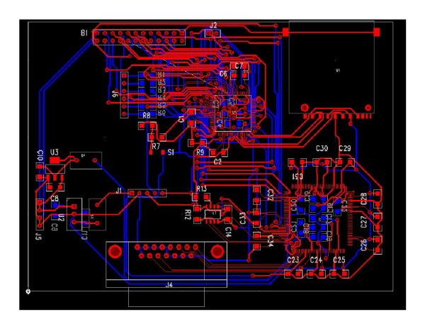
I added the power supply schematic as a new sheet in the PADS mainboard schematic. PADS already had PCB footprints for the regulators, and a 0.1″ header will be used to connect to the AC/DC converter card. I created a custom footprint for the current limiters, which was just 2 plated through holes spaced according to the datasheet. I noticed that the 3.3V regulator was only rated for 250mA, which may not be adequate given all of the 3.3V parts. I placed all of the footprints on a preliminary board layout for the TCSP and looked at different layout possibilities to minimize trace length and reduce the number of vias. The correct PCB footprint for the FPGA is yet to be determined.
February 24, 2010 (12 hours):
I spoke with Dhruv after the TCSP presentation and we decided that the voltage regulators would be in drop-out since they were being supplied by switching voltage supplies with exactly 3.3V and 5V outputs in the current design. The voltage regulators need an input voltage that is higher than the output voltage, so the 3.3V switching regulator will be removed from the design and the 5V AC/DC converter will supply the 5V rail. This should be fine since the only 5V part is the touch screen, and it has a 3.3V regulator on board. I added up the power requirements for all of the parts we have so far, and found that our current 3.3V regulator does not supply enough current to make me feel comfortable with it. I found another 3.3V regulator from Microchip which uses the 3 lead TO-220 package, which is a very standard package and pin-out for voltage regulators, including some already in lab.
With these changes, I redrew the power supply schematic and linked the components to PCB footprints in PADS.
Luke determined exactly which FPGA package we will be needing for our design, and I found pinout descriptions on the Altera website. I updated our schematic to reflect the recommended capacitor placements and power requirements of the FPGA. The core voltage of the FPGA is 1.2V, instead of 3.3V, so another regulator was added to the power supply circuit. I also changed the PCB footprint linked to the schematic for the FPGA.
February 25, 2010 (11 hours):
Today I created a new PCB layout, again taking trace length and the number of vias into account. I used the 1206 package for all of the capacitors and resistors, which is surface mount, and placed all of the bypass capacitors on the bottom layer, underneath the supplied IC whenever possible. For both the microcontroller and FPGA, the capacitors were specified to be within 1/4″ of the power and ground pins. The FPGA was very difficult to fit all of the capacitors next to and run all of the traces to the power and ground pins, especially since there are two power nets on the FPGA. Once all of the bypass capacitors were placed, I ran the power and ground traces first, with an effort to minimize the size of current loops on the board since these would create noise in the data lines. I also avoided making right angles whenever possible, which could create manufacturing problems. For the sake of time, and because I know more design changes are coming, I autorouted the rest of the traces. This will be inadequate for the final design, since the autorouter does not make very smart decisions when it comes to the previously mentioned considerations.
WEEK 07 SUMMARY
Accomplishments:
Weekly Work Total: 40 hours
Project Work Total: 102 hours
Week 08
March 2 (10 hours):
The FPGA is capable of doing much more than what we need it to do (displaying a static VGA image). So, since the image we are displaying is static and very simple, we will generate our own VGA signals and get rid of the FPGA, since it would require another programmer, a 1.2V power supply net, and quite a bit of real estate on the PCB to do a very simple task. Luke and Ethan created a block diagram and a new list of parts for the VGA circuit, which I used to update the schematic and PCB footprints in my PADS library.
In addition to the components indicated in the block diagram, I added a level translator recommended by Chuck to interface the 3.3V logic of the SRAM IC to the 5V logic of the PLDs, which will generate the sync pulses.
The new schematic for the VGA circuit is as follows:
With the FPGA now removed from the design, the 1.2V regulator is no longer necessary. The current limiters were also removed from the power supply design since they weren’t necessary, resulting in the following design:
Once the schematic was updated, the new netlist was pushed to PADS Layout, and a new PCB layout was created. Again, I manually rounted the power and ground traces to ensure that current loops were minimized, and manually connected the bypass capacitors to the appropriate power and ground pins on all of the ICs. Once this was done, I autorouted the rest of the traces since a few more modifications to the VGA circuit are still being discussed.
For more detail: Andy Robison’s Lab Notebook