An innovative architectural approach is required to manage multi-hundred gigabit-per-second levels of system performance with smart processing at full line rate, scaling to terabits and teraflops.
The mandate isn’t simply to increase the performance of each transistor or system block, or scale the number of blocks in the system, but to fundamentally improve the communication, clocking, critical paths, and interconnect to address the massive data flow and intelligent packet, DSP, and/or image processing at line rates.
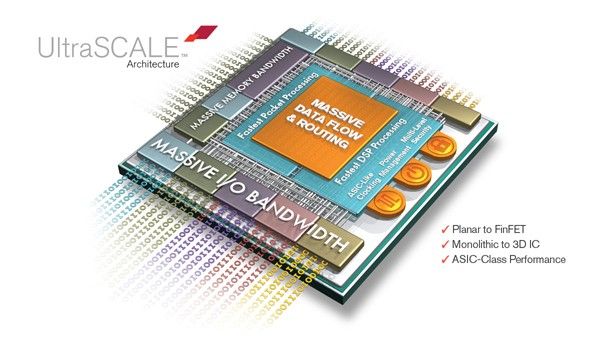
The UltraScale™ architecture addresses these challenges by applying leading-edge ASIC techniques in a fully programmable architecture. This architecture scales from 20nm planar through 16nm FinFET technologies and beyond, while also scaling from monolithic through 3D ICs. It not only addresses the limitations to scalability of total system throughput and latency, but directly addresses interconnect — the number one bottleneck to system performance at advanced nodes.
- Massive data flow optimized for wide busses supporting multi-terabit throughput with lowest latency
- Highly optimized critical paths and built-in high-speed memory cascading to remove bottlenecks in DSP and packet processing
- Enhanced DSP slices incorporating 27×18-bit multipliers and dual adders that enable a massive jump in fixed- and IEEE Std 754 floating-point arithmetic performance and efficiency
- Step function in inter-die bandwidth for 2nd generation 3D IC systems integration and new 3D IC wide memory optimized interface
- Massive I/O and memory bandwidth, including support for next-generation memory interfacing with dramatic latency reduction and multiple hardened, ASIC-class 100G Ethernet, Interlaken, and PCIe® IP cores
For more detail: Xilinx ships first 20nm Asic-like FPGA