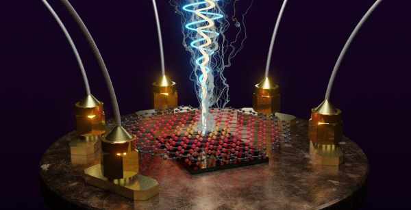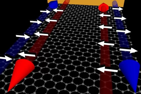
NEW STUDY SHOWS RARE FORM OF MAGNETIC AND ELECTRICAL PROPERTY IN STACK-TWISTED GRAPHENE
A group of scientists at Columbia University and the University of Washington has found unique electronic states along with an uncommon kind of magnetism, can develop in a three-layer graphene structure. The work was inspired by current research studies of twisted monolayers or twisted bilayers of graphene, making up either 2 or 4 overall sheets. These results were discovered to treat […]
NEW STUDY SHOWS RARE FORM OF MAGNETIC AND ELECTRICAL PROPERTY IN STACK-TWISTED GRAPHENE Read More »