Summary of Reverse Engineering a NAND Flash Device Management Algorithm
Summary: The author recovered data from a physically damaged SD card by reverse-engineering the on-flash format and NAND device management. After finding the storage IC intact, they studied differences between NOR and NAND flash, explained NAND's serialized command interface, error and wear constraints, and outlined the three core NAND management tasks: data decorrelation, error correction, and wear-leveling. Their month-and-a-half effort (plus longer follow-up) resulted in full recovery of photos and videos.
Parts used in the SD card recovery project:
- Damaged SD card (with removed or broken plastic housing)
- SD card main PCB (with controller and flash IC)
- Flash memory IC (NAND flash chip from the SD card)
- Silicon Motion SM2683EN controller (on the SD card PCB)
- Soldering tools for desoldering the flash IC
- Hardware for interfacing with the raw flash IC (e.g., adapter or socket)
- Data capture tools to read raw NAND flash contents
- Reverse-engineering software and source code (for on-flash format and device management)
- Photos of hardware (documentation resources)
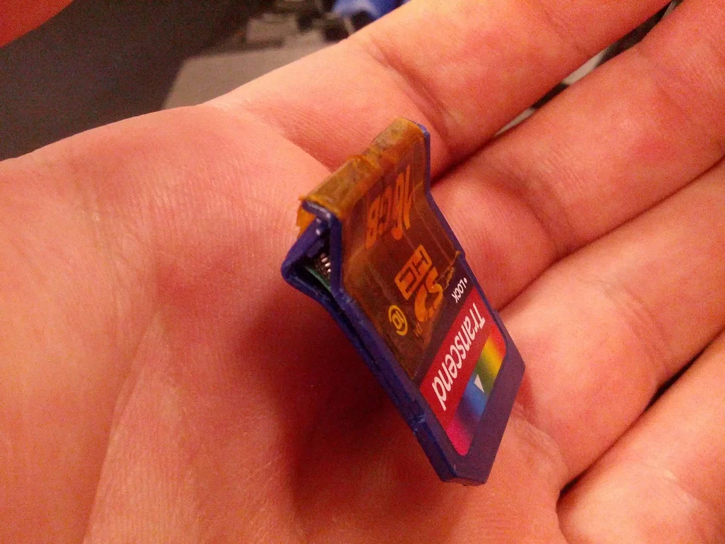
Around June of 2012, I had gotten myself into a very bad habit. Instead of carrying my SD card in my camera, I left it sticking out of the side of my laptop, presumably intending to do something with the photos on it eventually. On my flight home from Boston, the predictable thing happened: as I got up out of my seat, the machine fell out of my lap, and as the machine hit the ground, the SD card hit first, and was destroyed.
I was otherwise ready to write off the data stored on that device, but something inside me just wasn’t happy with that outcome. Before I pitched the SD card in the trash, I took a look at what remained – as far as I could tell, although the board was badly damaged, the storage IC itself was fully intact (although with a few bent pins).
The following is a description of how I went about reverse-engineering the on-flash format, and of the conclusions that I came to. My efforts over the course of about a month and a half of solid work – and a “long tail” of another five months or so – resulted in a full recovery of all pictures and videos that were stored on the SD card.
If you’re just looking for the resources that go with this project, here are the pictures of the hardware, and here is the source code.
You can discuss this article on Hacker News.
Introduction
It is probably fitting to start with a motivation for why this problem is complex; doing data recovery from a mass-production SD card seems like it should be a trivial operation (especially given the interface that SD cards present), but as will become clear, it is not. From there, I will discuss the different parts of the problem in detail, both in terms of how they physically work, and in terms of what it means from the standpoint of a data recovery engineer.
I begin with a brief history of the field. In the past ten years, solid-state data storage has become increasingly complex. Although flash memory was originally commercialized in 1988, it only began taking off as consumer mass storage recently. In August of 2000, COMPAQ (and later, HP) began producing the iPAQ h3100/h3600 series of handheld computers, which had between 16 and 64MB of flash memory. This was approximately a standard capacity for the time period; the underlying technology of the flash device was called ”NOR flash”, because of how the memory array was structured. NOR flash, in many regards, behaved like classic ROM or SRAM memories: it had a parallel bus of address pins, and it would return data on the bus I/O pins in a fixed amount of time. The only spanner in the works was that writes could only change bits that were previously ones to zeroes; in order to change a zero back to a one, a whole block of bits (generally, around 16 KBytes) had to be erased at once.
This was okay, though, and we learned to work around these issues. NOR flash had a limited erase life – perhaps only some millions of erases per block – so filesystems on the device generally needed to be specially designed to “wear-level” (i.e., scatter their writes around the device) in order to avoid burning an unusable hole in the flash array. Even still, it still appeared a lot like a block device that operating systems knew how to deal with; indeed, since it looked so much like SRAM, it was possible to boot from it on an embedded system, given appropriate connections of the bus pins.
Around 2005, however, NOR flash ran into something of a problem – it stopped scaling. As the flash arrays became larger, the decode logic began to occupy more of the cell space; further, NOR flash is only about 60% as efficient (in terms of bits per surface area) as its successor. To continue a Moore’s Law-type expansion of bits per flash IC, flash manufacturers went to a technology called NAND flash. Unfortunately, as much as it sounds like the difference between NOR flash and NAND flash would be entirely internal to the array, it isn’t: the external interface, and characteristics of the device, changed radically.
As easy as NOR flash is to work with, NAND flash is a pain. NOR flash has a parallel bus in which reads can be executed on a word-level; NAND flash is operated on with a small 8-bit wide bus in which commands are serialized, and then responses are streamed out after some delay. NOR flash has an amazing cycle life of millions of erases per block; modern NAND flashes may permit only tens of thousands, if that. NOR flash has small erase blocks of some kilobytes; NAND flash can have erase blocks of some megabytes. NOR flash allows arbitrary data to be written; NAND flash imposes constraints on correlating data between adjacent pages. Perhaps most distressingly of all, NOR flash guarantees that the system can read back the data that was written; NAND flash permits corruption of a percentage of bits.
In short, where NOR flash required simply a wear-leveling algorithm, modern NAND flash requires a full device-management algorithm. The basic premises of any NAND device-management algorithm are three pieces: data decorrelation (sometimes referred to as entropy distribution), error correction, and finally, wear-leveling. Oftentimes, the device management algorithms are built into controllers that emulate a simpler (block-like) interface; the Silicon Motion SM2683EN that was in my damaged card is marketed as a “all-in-one” SD-to-NAND controller.
For more detail: Reverse Engineering a NAND Flash Device Management Algorithm
- How was the SD card physically damaged?
The laptop fell and the SD card hit the ground first, destroying the card. - Was the flash storage IC intact after the damage?
Yes, the board was badly damaged but the storage IC appeared fully intact with a few bent pins. - What was the end result of the recovery effort?
The author achieved a full recovery of all pictures and videos stored on the SD card. - Why is NAND flash more difficult to recover data from than NOR flash?
NAND flash uses a serialized command interface, has larger erase blocks, lower cycle life, correlation constraints between pages, and permits some bit corruption, requiring full device-management algorithms. - What are the three core pieces of a NAND device-management algorithm?
Data decorrelation (entropy distribution), error correction, and wear-leveling. - What controller was on the damaged SD card?
The card used a Silicon Motion SM2683EN SD-to-NAND controller. - Did the author provide resources or source code for the project?
Yes, the article links to pictures of the hardware and the source code used in the project. - How long did the main recovery work take?
About a month and a half of solid work, plus a long tail of another five months.