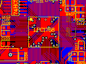
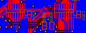
The electronics industry is evolving at a fast pace, with IoT and wearable devices driving the trend. This calls for smaller PCB that packs more features than before. In these devices, the PCB must be designed for SMT assembly and they should adhere to best design practices to minimize defects in final products.
Best Design Practices For SMT Assembly
Before you start manufacturing your PCB, do ensure that it is optimized for SMT assembly. Here are a few helpful tips.
- Fiducial markers – Ensure that global fiducial markers are in place for proper and accurate components placement of the assembly machines. If your design consists of Quad Package surface mount components like QFP, QFN or BGA, do check with your SMT assemblysuppliers if you need to include local fiducials as well.
- Mask Vias Under BGA
If your design contains BGA components, ensure that any vias that are beneath the component are properly masked. This prevents the solder ball from touching or smearing on the via and create unintended connections that are unable to spot visually.
- Components Placement.
Basic guidelines of components placement must be adhered not only for the sake of SMT assembly but also for troubleshooting purpose down the line. Components should be aligned and maintain similar orientation throughout the design.
For more detail: How To Prepare Your PCB For SMT Assembly


