PIC12 ADC Converter using PIC12C671 with Proteus Simulation

Summary of PIC12 ADC Converter using PIC12C671 with Proteus Simulation


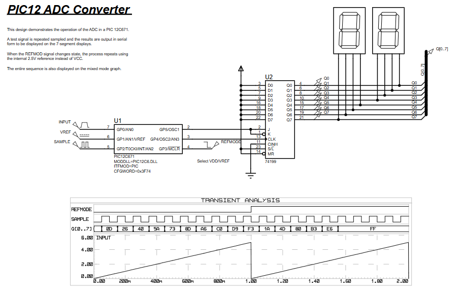
The PIC12 ADC Converter project demonstrates using the PIC12C671 internal ADC to sample an analog input, convert it to an 8-bit value, and serially shift that result out to external latch and dual 7-segment displays. It supports runtime selection of VDD or external VREF, uses interrupt-driven ADC completion, and is fully simulated in Proteus for visualization and learning.

Parts used in the PIC12 ADC Converter:

  • PIC12C671 microcontroller
  • External voltage reference source (VREF)
  • Serial latch IC
  • Dual 7-segment displays
  • Clock and sample control signal sources
  • Proteus VSM environment for simulation
Introduction

The PIC12 ADC Converter project demonstrates how the built-in analog-to-digital converter (ADC) of the PIC12C671 microcontroller works in a practical setup.
An analog input signal is repeatedly sampled, converted into digital form, and then sent out serially for visual representation.
This project is ideal for learning ADC fundamentals using a microcontroller project simulated in Proteus simulation.
It clearly shows how reference voltage selection affects conversion results.
The design is compact, educational, and well-suited for embedded systems and DIY electronics learning.

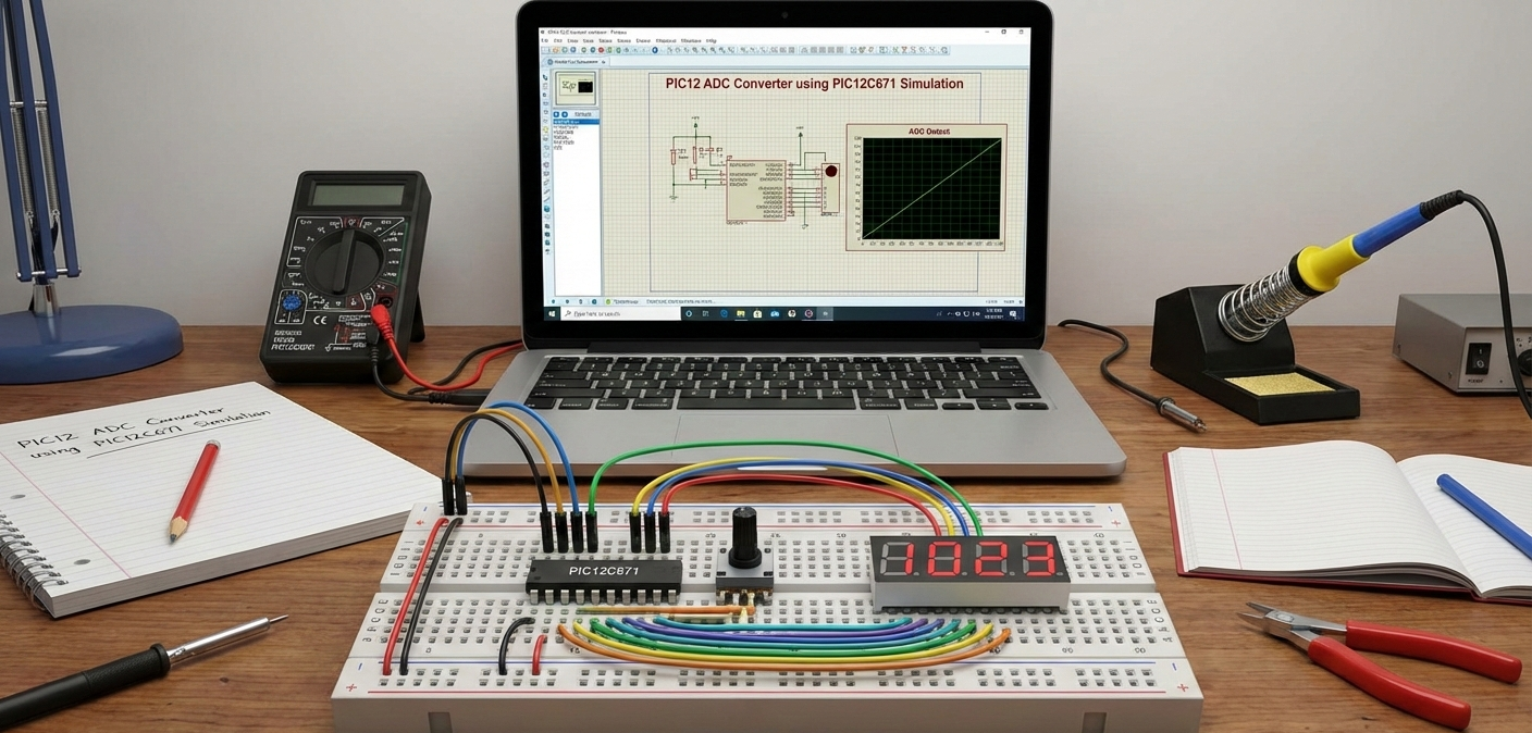
PIC12 ADC Converter Setup
Illustrative View of the Concept.

How the Project Works (Overview)

The PIC12C671 samples an analog voltage applied to its input pin and converts it into an 8-bit digital value using its internal ADC.
The converted result is then shifted out bit-by-bit through GPIO pins and displayed externally using a latch and 7-segment displays.
The ADC can operate with either VDD or an external VREF, selectable during runtime using a control signal.
All signal activity and conversion behavior are visible in Proteus through transient analysis graphs.

Block Diagram / Workflow Explanation

  1. Analog Input Signal is applied to the ADC input pin

  2. ADC Module (PIC12C671) samples and converts the signal

  3. Reference Voltage Selection switches between VDD and external VREF

  4. ADC Result Register (ADRES) stores the conversion value

  5. Serial Output Logic shifts data bit-by-bit via GPIO

  6. External Latch & Displays show the converted value

  7. Proteus Graph visualizes voltage and conversion results

Key Features

  • Uses internal ADC of PIC12C671 microcontroller

  • Runtime selection of voltage reference (VDD or external VREF)

  • Serial output of ADC result without dedicated UART

  • Interrupt-driven ADC completion handling

  • Visual display using 7-segment outputs

  • Fully simulated using Proteus VSM

Components Used

  • PIC12C671 microcontroller

  • External voltage reference source

  • Serial latch IC

  • Dual 7-segment displays

  • Clock and sample control signals

  • Proteus VSM environment

Applications

  • Learning ADC working principle in microcontrollers

  • Embedded systems education and training

  • Sensor interfacing experiments

  • Low-pin-count microcontroller projects

  • ADC reference voltage comparison studies

  • Firmware testing using Proteus simulation

Explanation of Code (High-Level)

The firmware initializes the ADC module and GPIO configuration.
An external interrupt wakes the MCU from sleep to begin sampling.
The ADC reference source is selected dynamically based on input state.
After acquisition delay, conversion starts and completion triggers an interrupt.
The ADC result is read from ADRES and serialized bit-by-bit using GPIO pins.
Clock pulses are generated manually to shift data to the external display logic.

Source Code

Download
       LIST    p=12C671 ; 
	#include "P12C671.INC" ; Include header file

; Macro to generate a MOVLW instruction that also causes a model break:
break   MACRO arg
        DW    0x3100 | (arg & H'FF')
        ENDM

bank0   MACRO 
	bcf STATUS,RP0
	ENDM
	
bank1   MACRO
	bsf STATUS,RP0
	ENDM	

Proteus Simulation

In Proteus, the analog input ramps smoothly while ADC sampling occurs periodically.
The converted digital values update in real time and appear on the 7-segment displays.
Switching the reference voltage clearly changes the conversion scale.
The transient graph shows ADC response aligned with input voltage changes.

(FAQs)

1: Why use PIC12C671 for ADC projects?

It provides a simple ADC module with minimal pin usage, ideal for learning.

2: Can this work with other PIC12 devices?

Yes, with minor ADC register and pin configuration changes.

3: Why is sleep mode used frequently?

It reduces power usage and waits efficiently for interrupts.

4: How is serial output implemented without UART?

GPIO pins manually shift data using clock pulses.

5: Can I display ADC data differently?

Yes, LCDs or LEDs can be used instead of 7-segment displays.

6: Why does reference voltage matter?

It defines the ADC conversion range and resolution.

7: Is this suitable for real hardware testing?

Yes, the logic directly maps to real PIC12C671 hardware.

Conclusion

The PIC12 ADC Converter project is a compact and effective way to understand ADC operation in microcontrollers.
It combines firmware, hardware logic, and Proteus simulation into a clear learning experience.
This project strengthens core skills in embedded systems, ADC handling, and serial data transfer.
A solid foundation project for anyone exploring practical electronics and firmware design.

Quick Solutions to Questions related to PIC12 ADC Converter:

  • Why use PIC12C671 for ADC projects?
    Because it provides a simple ADC module with minimal pin usage, making it ideal for learning.
  • Can this work with other PIC12 devices?
    Yes, with minor ADC register and pin configuration changes.
  • Why is sleep mode used frequently?
    It reduces power usage and lets the MCU wait efficiently for interrupts.
  • How is serial output implemented without UART?
    GPIO pins manually shift data bit-by-bit using generated clock pulses.
  • Can I display ADC data differently?
    Yes, LCDs or LEDs can be used instead of 7-segment displays.
  • Why does reference voltage matter?
    It defines the ADC conversion range and affects conversion results.
  • Is this suitable for real hardware testing?
    Yes, the logic directly maps to real PIC12C671 hardware.

About The Author

Ibrar Ayyub

I am an experienced technical writer holding a Master's degree in computer science from BZU Multan, Pakistan University. With a background spanning various industries, particularly in home automation and engineering, I have honed my skills in crafting clear and concise content. Proficient in leveraging infographics and diagrams, I strive to simplify complex concepts for readers. My strength lies in thorough research and presenting information in a structured and logical format.

Follow Us:
LinkedinTwitter