Summary of PIC based UPS Schematic / Firmware / PCB Layout
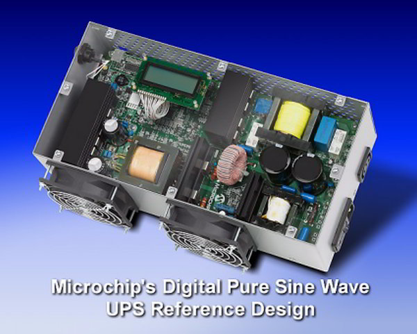
Microchip’s Digital Pure Sine Wave UPS reference design uses dsPIC33F GS digital-power DSCs to implement a 1 kVA (1350 VA peak) pure sine-wave UPS with high-frequency topology, intelligent battery charging, USB communication, LCD front panel, and royalty-free complete documentation, firmware, and hardware. It features a push-pull DC-DC, full-bridge inverter with unipolar sine-triangle PWM, and a flyback switch-mode battery charger, enabling compact, efficient, low-noise operation with adjustable charge current and fast mains-to-battery transfer.
Parts used in the Digital Pure Sine Wave UPS Reference Design:
- dsPIC33F GS series digital-power DSC (controller)
- MOSFETs for push-pull converter
- IGBT modules for full-bridge inverter
- Transformer/magnetics for push-pull step-up
- DC link capacitors (to achieve ~390 VDC)
- Output filter components (inductors and capacitors)
- Flyback converter components (transformer, switch, diodes)
- Battery: 36 V (3 × 12 V lead-acid)
- Battery charging circuit components (sensing resistors, current sensors)
- Heat sink and temperature sensor
- USB interface hardware
- LCD front-panel display
- Protection and sensing components (voltage/current sensors, fault indicators)
- PCB and connectors
Microchip’s Digital Pure Sine Wave Uninterruptible Power Supply (UPS) Reference Design is based on the dsPIC33F “GS” series of digital-power Digital Signal Controllers (DSCs). This reference design demonstrates how digital-power techniques when applied to UPS applications enable easy modifications through software, the use of smaller magnetics, intelligent battery charging, higher efficiency, compact designs, reduction in audible and electrical noise via a purer sine-wave output, USB communication and low-cost overall bill-of-materials. This reference design is Royalty Free. This project contains complete documentation and software & hardware design information.
UPS Input / Output Specifications:Input Range AC:
Output Voltage AC:
DC Input:
Rating:
|
UPS Features:
- High-frequency design
- Adjustable Charging current
- Efficiency of 84%
- Pure sine wave output with THD <3%
- Mains to Battery Transfer time < 10 ms
- Supports Crest Factor of 3:1
- Minimum Power Factor(Leading/Lagging) of 0.65
- Fault indications
- USB Communication with PC
- LCD front panel
The Digital Pure Sine Wave UPS System operates in two modes:
Standby Mode – Operational in the presence of AC line voltage; battery is charged in this mode.
UPS Mode – Operational during power outage; the system switches to a function called inverter to provide power to load. Charge stored in the battery is converted to AC output.
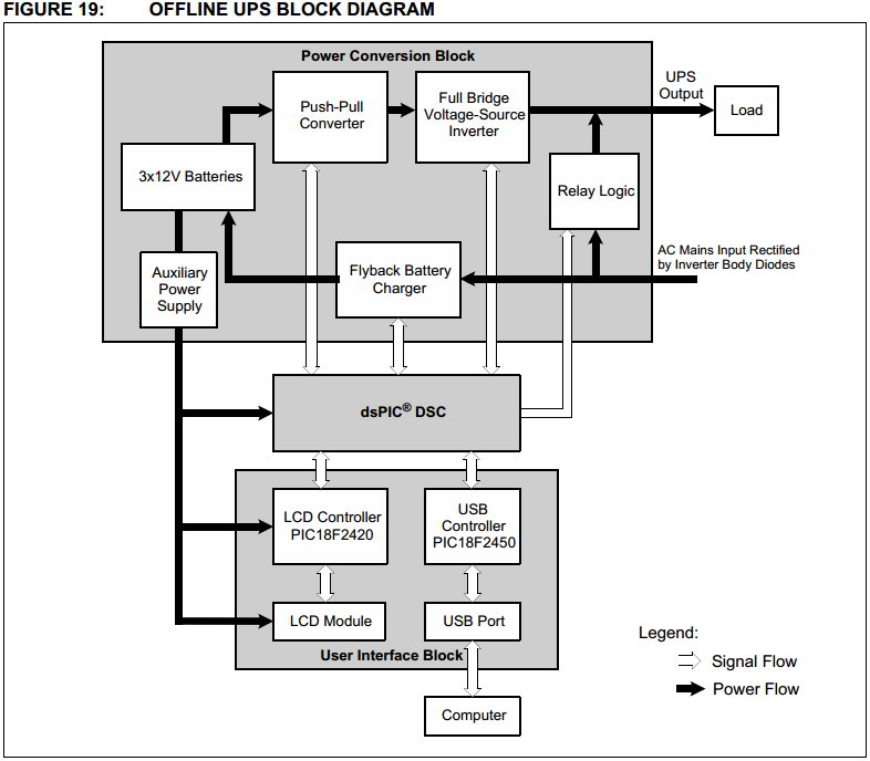
The Digital Pure Sine Wave UPS System has three power conversion stages:
PUSH-PULL CONVERTER:
The push-pull converter steps up the battery voltage to 390 VDC. After enabling the MOSFET driver, the PWM outputs from dsPIC® DSC control the output voltage. Input and output DC voltage, primary current and heat sink temperature act as feedback signals.
FULL-BRIDGE INVERTER
A full-bridge inverter topology is used to convert the high-voltage DC to pure sine AC output. Sine-triangle PWM in unipolar configuration is used to switch inverter IGBT modules. Full-bridge with unipolar switching helps to optimize components rating, and reduces output filter size. Input DC voltage, output AC voltage, output filter current and incoming line AC voltage are used as feedback signals to implement efficient full-bridge control loop. Fast and intelligent switch-over from “Mains” to “Inverter” and vice versa is implemented with intelligent switchover algorithm, which also helps to control in-rush current during switchovers.
FLYBACK SWITCH MODE CHARGER
Flyback converter is used for battery charging to prevent charging losses over other methods. In the presence of AC mains voltage, the Inverter mode is disabled, and the UPS switches to the battery charging mode. The dsPIC®DSC device provides the reference current level with a variable duty cycle PWM signal. Battery voltage and battery charging current are used as feedback signals to implement an intelligent charging profile, which extends the battery life.
Block Diagram of UPS – Shows Functionality & Basic Flow
UPS Schematic 1 out of 8
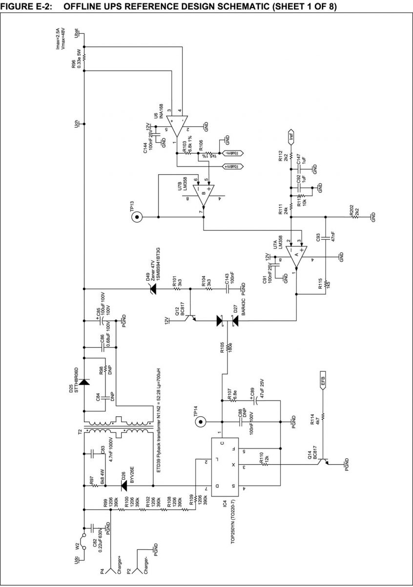
for Firmware, detailed schematic & other details visit: Pic Based Pure Sinewave UPS
Source: PIC based UPS Schematic / Firmware / PCB Layout
- What controller is used in the UPS reference design?
The design uses the dsPIC33F GS series digital-power DSC. - What is the steady-state and peak power rating of the UPS?
The UPS is rated at 1000 VA steady-state and 1350 VA peak (surge). - What battery configuration does the UPS use?
The UPS uses a 36 V DC battery made of three 12 V lead-acid batteries in series. - What three power conversion stages are implemented?
Push-pull converter, full-bridge inverter, and flyback switch-mode charger. - What switching method is used for the inverter?
Sine-triangle PWM in unipolar configuration is used to switch the inverter IGBT modules. - How fast is the transfer from mains to battery?
Mains to battery transfer time is less than 10 ms. - What is the UPS output waveform quality?
The design provides a pure sine wave output with total harmonic distortion less than 3%. - Does the design support communication with a PC?
Yes, it supports USB communication with a PC. - What efficiency is claimed for the UPS?
The UPS has an efficiency of 84%. - Is the reference design documentation and firmware available royalty free?
Yes, the reference design is provided royalty free with complete documentation, software, and hardware design information.